Common Soldering Process Issues

Oxidization
Fast oxidisation is a common issue related to high temperatures and presence of oxygen during the convection reflow or wave soldering processes. The oxidisation may induce some degradation of metal surface and its environmental robustness, thus impacting the components and the electronic hardware lifetime.
The level of oxidisation is depending on more factors, the second most important (after the degree of temperature itself) is a selection of activation flux that is part of the solder paste. More “aggressive” flux is improving the solder wetting and solder joint strength, on the other hand it is increasing oxidisation and require thorough cleaning process to remove all flux residual. Despite, common practise, most component manufacturers do not recommend use of highly activated fluxes due to this reason.
Soldering in an inert gas atmosphere, typically nitrogen, can be recommended to avoid use of highly activated fluxes and as a way to suppress amount of oxygen present during the soldering process. The use of nitrogen also significantly increases the wetting force and thus it improves solder joint quality. Of course, the main down side is increase of the mounting process cost.
Component displacement
Some component displacement may occur during board mounting, especially during mass production using convection IR reflow oven. The component displacement is caused by changes of surface tension during the thermal flow. The component moves to a position with “minimal energy” that can be observed as:
Component self-alignment – in case of correct PCB pad design and uniform thermal profile, the component is self-centred on the position – this is ideal, target stage of the right mounting process and PCB layout design set up.
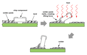
Skewed “swimming” components or tombstoning (‘Manhattan effect’, ‘drawbridging’, or ‘Stonehenge effect’)
During the component “swimming” displacement, the mounted parts are skewed outside of their PCB pads centre position. “Tombstoning” effect happens, when one component side is lifted upwards (see drawing). These faulty component placement phenomena are caused by uneven wetting forces between the component sides during soldering. There are number of factors that are influencing these issues, such as:
- different heat capacity connected to the pads
- pad design layout and position
- solder paste printing mis-alignment
- Wettability differences between the two terminations
- faulty solder paste application
- faulty pick and place process pushing one termination stronger inside the solder paste
- misaligned component placement
Tombstoning occurs more frequent with short, wide terminations, and with thin & light devices such as miniature capacitors and resistors. The wetting forces vary with chip dimensions; the downward forces vary with the square of the chip dimensions.
Outgassing
Non-hermetic, epoxy based packages used by number of component designs are featuring a micro porous structure that may act as a moisture residuals traps. While, the components itself are designed and constructed to operate reliably in accordance to their specifications, some outgassing and fast moisture evaporation can occur during the high temperature board mounting process.
Outgassing itself may not present a danger for the components itself, if the reflow conditions such as preheat and temperature gradients are within the manufacturer specifications. However, the issue arises for high density mounted PCBs, where small & light components are placed very close to large components. Outgassing from large components can blow out and displace nearby small parts in this case. As an example 7343 SMD chip tantalum capacitors can blow out small 0201 MLCC capacitors placed very closed to the capacitor body.
The prevention and recommendation especially for highly populated PCBs would be to use dry packed components or use appropriate pre-dry process to remove maximum moisture out of the components packaging.
Sulfur Contamination
Sulfur contamination is mainly associated with use and reliability of thick-film chip resistor with Ag-system as inner termination. The silver in the inner termination is very susceptible to contamination via sulfur which produces silver sulfide in chip resistors. Silver is so susceptible to combination with sulfur that the sulfur diffuses through the outer termination layers to the inner termination forming silver sulfide. Silver sulfide unfortunately makes the termination material non-conductive and effectively raises the resistance value until it is essentially open circuit. The reaction velocity in this case is influenced by sulfur gas density, temperature and humidity greatly. This process can be initiated or inhibited already by heat-stress while mounting.

Sulfur can be found in various types of oils and lubricants, rubber gaskets, hoses, belts, and grommets, connectors, and in some applications in the very air that the electronic device operates in. Silver sulfide contamination is a latent failure mode that is undetectable at the time the resistor is manufactured and when the resistor is mounted into its electrical circuit.
Factors such as incomplete or misaligned passivation, incomplete plating, and using low palladium materials for the inner termination, can accelerate the formation of silver sulfide on the chip and lead to failure much faster than would be expected. There are remedies for each of these issues, but all involve increased manufacturing cost which is never popular when considering thick film commodity chip resistors. [16]
Inert gas atmosphere mounting (as mentioned in this chapter above) can be recommended as a prevention measure to suppress the sulfide contamination issues.
General Measures to Enhance Components’ Soldering and Mounting Capabilities
TCE mismatch presents one of the key component construction challenges to manufacturers. Selection and development of right materials are key for balance between robustness, specification and cost, thus it can be one of the main differentiator between products for different applications, temperature range and reliability levels.

- TCE mismatch ready, proper material selection
- termination solder finish type
- anti-migration barriers
- moisture barriers (impregnation)
- dry packaging
- post-reflow treatment – ageing recommendation
The termination solder finish is depending on mounting process (see the previous chapter) and solder type (SnPb/leadfree ….). Anti-migration termination sub-layers are used to supress diffusion and oxidisation processes that may degrade terminations solderability during storage. The selection of the anti-migration layers depends on lead types and components. Nickel layer is commonly used as an excellent diffusion barrier, however it is brittle in thick layers, thus with flat terminations such as MLCC chip capacitor, it is used with 1-2mm thickness, while on “bended J-lead” tantalum terminations nickel thickness is just 0.1-0.2 mm, as thicker nickel would crack in bend area resulting in diffusion, growth of intermetallic alloys and loss of solderability.
Moisture, together with temperature and voltage is one of the main accelerating factors for diffusion and oxidisation degrading process. Thus many components are today using some form of moisture barriers such as silicon/oil impregnation or dry packing. Dry packing can be recommended as a preventive measure to suppress mounting thermal issues on all components. Where dry packing cannot be used or it is not practical, some components pre-dry process prior mounting would be recommended in order to suppress the component history/storage/manufacturing moisture related variation.