PCB Board Design and Handling
Board Design and Component Pre-Assembly Preparation
The leads of leaded components shall be bent and often cut to the right length before they are mounted / soldered to the substrate. Lead cutting, bending and mounting are operations that may be hazardous if they are not performed properly.
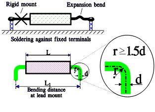
Components mounted to soldering terminals must be provided with a small expansion bend on the leads (Figure 10). Otherwise we shall run the risk that temperature dependent contractive forces will be transferred to internal contact areas causing them to fracture and create an open circuit. This kind of an open circuit usually appears intermittently and is, of course, temperature dependent; that will make the trouble shooting difficult and uncertain.
When the connecting leads are bent it has to be done according to specific rules. If we bend too close to the component body, we run a great risk of transferring forces to internal connections that could be damaged. The forces may also cause cracks in hermetic seals. With Figure 8. as a starting point we can write the following equation:
L + 3d <= n x M = L1 ………………………………….Eq. [1]
, where n is the lowest possible integer fulfilling Equation 1. M stands for used modulus of the board layout, 2.5 or 2.54 mm. For small component bodies sometimes half the modulus needs to be used in order not to make the bending distances unnecessarily large. With large bodies standardizing may justify that n is limited only to odd values. Capacitors and magnetic devices (no heat produced) heavier than 5 – 10 gram should be fixed mechanically attached to the substrate.
If power leaded components are soldered to turrets as shown in the top example of Figure 10. we have to ensure that the heat transfer through the leads doesn’t melt the solder. In critical cases it may be necessary to choose longer or thinner leads, less heat conductive lead material or, alternatively, we must decrease the power developed in the component or bond it to the PCB with a thermal adhesive.
We must also see to it that the height over the substrate is adequate with respect to allowing sufficient thermal radiation. Heat from the soldering process may, in unfortunate cases, be conducted up through the leads melting the internal solder connections in radial lead components that are mounted close to the circuit board. To avoid this, we should ensure that those connections are made with a high-temperature solder.
Cutting a component lead with side cutting pliers will expose the component to a considerable mechanical shock. This applies also to automatic lead cutters. The shock is of short duration and the magnitude may vary strongly from one type and manufacture to another. If such components are used whose construction may be sensitive to mechanical shocks, the mechanical forces should be measured and the exposure to the cutting forces evaluated. A cutting plier with a flat edge toward the component reduce this shock.
Mounting considerations for single-ended components
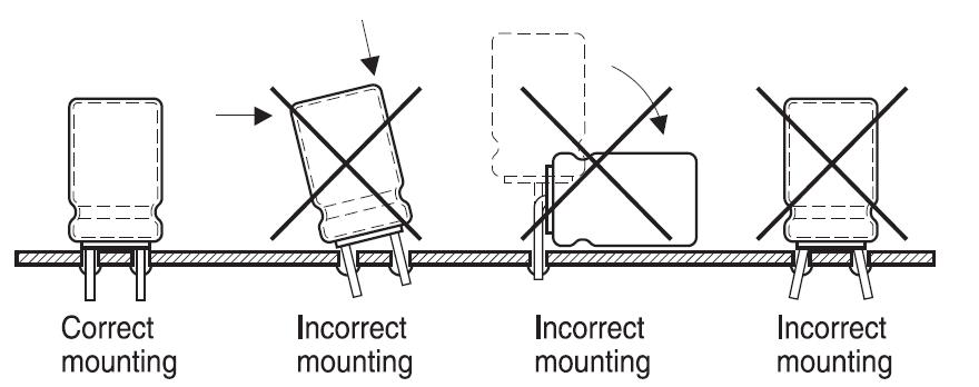
The internal structure of single-ended components might be damaged if excessive force is applied to the lead wires. Stresses like push, pull, bend etc. might cause electrical parameters deterioration or open/short circuit, due to rupture of terminals or internal elements.
Pay attention to the following cautions:
- Do not move the component after soldering to PC board.
- Do not pick up the PC board by holding the soldered component.
- Do not insert component on the PC board with a hole space different to specified lead space.
- Check the recommended component position into consideration when designing the PC board layout.
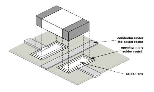
SMD component pads
should be designed to achieve good solder filets and minimize component movement during reflow soldering. Pad designs – see manufacturer’s datasheets for pad design recommendations. The basis +of these designs may include:
- Pad width equal to component width. It is permissible to decrease this to as low as
85% of component width but it is not advisable to go below this.
- Pad overlap 0.5mm beneath component.
- Pad extension 0.5mm beyond components for reflow and 1.0mm for wave soldering.
Some common pad design related mounting problems and recommendations are shown in Fig.12. Below.
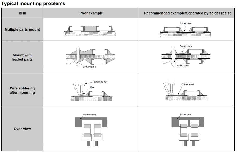
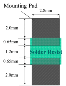
The correct layout of solder resist, as used in Figure 12. examples, can mitigate certain mounting issues. See Fig.13. solder resist layout design example on SMD component.
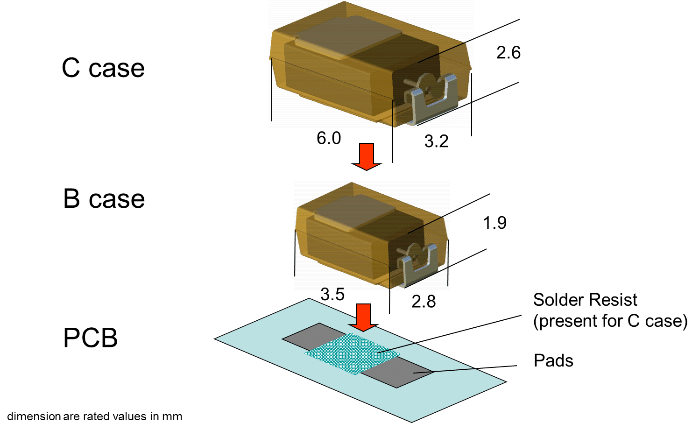
Solder resist can be used also in some cases to modify pad design in relative inexpensive way to adjust to new component or fix a pad layout issue. A flexible pad design concept using solder resist masking that allows flexible replacement of C and B case tantalum capacitors was suggested by AVX – see Fig.14. Smaller B case size can offer cost saving over larger C case size when it is available / qualified without need of expensive circuit board pad re-design.
It is important to remember that SMD components, more than the others, are influenced by temperature changes, especially for the larger component. Thus, dimensions and mounting directions are most important. Further, short and wide bodies are preferable to long and thin ones, partly for strength reasons, partly because of the inductance and with that the frequency dependence will decrease. Still another reason is that constraint density in solder joint from coefficient of expansion between substrate and chip decreases in significance with shorter distances between terminations. This approach results in a strongly improved mechanical strength, better electrical parameters and thermal dissipation. This would be a typical recommendation for assembly of mechanically sensitive MLCC capacitors – see Fig.15. The same principle works on MLCC “reverse geometry” types, where the terminations are made alongside the longer dimension of the chip.
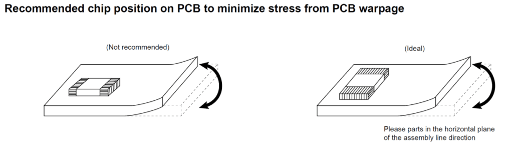
Since the stress to the curvature or bending at the time of breaking printed substrate, may cause fault when arranging surface mount components near printed substrate breaking point, consideration is required for the method of arrangement of surface mount components. (see also chapter 4.2.8.).
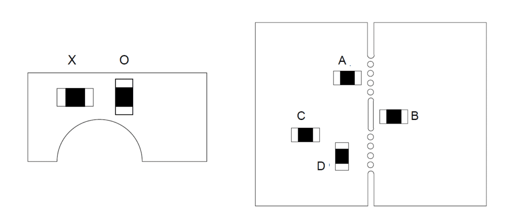
The above figure 16. Illustrates mechanical stress considerations related to the SMD component PCB layout orientation. Risk of mechanical issues on the Fig 16. right side can be assumed:
A > C > B >>>>>>>>>> D
Therefore, arrange to the break line of printed substrate as in parallel as possible, keep away from break line as much as possible or use milling machine/tool to perform the cut.
Passive components chips may produce also some heat and, to some extent, also SM magnetics. In comparison with lead mount components the heat conduction through the solder joints of the SMDs is good. Hence the relative temperature of the body centre with respect to non-SMDs will decrease and will rise in the solder joints. A wide lead pattern will facilitate the heat transfer still more. It will allow a larger electric load before we reach the specified ”hot spot” temperature. Nevertheless, the thermal dissipation and radiation has to be considered during the PCB and pad layout design.
Because of their size SMD styles always must be furnished with flexible leads in order to prevent damage during temperature cycles. Heavier components, in order to prevent them from coming loose when subjected to shock or vibration, should be mechanically attached to their substrate by means of an adhesive or staking compound.
Component Spacing
For wave soldering, components, must be spaced sufficiently far apart to avoid bridging or shadowing (inability of solder to penetrate properly into small spaces). This is less important for reflow soldering but sufficient space must be allowed to enable rework should it be required. At least 0.5 mm air space or additional insulation should separate components from adjacent metal parts, for example conductive patterns on printed circuit boards.
Component Handling
Commercial non-hermetic components should be handled with care to avoid damage or contamination from perspiration and skin oils. The use of tweezers or vacuum pick-ups is strongly recommended for individual components. Bulk handling should ensure that abrasion and mechanical shock are minimized. Taped and reeled components provides the ideal medium for direct presentation to the placement machine. Any mechanical shock should be minimized during handling of components, especially chip multilayer ceramic capacitors.
Multiple leads components (such as some SMD film capacitors, arrays etc.) terminations flatness shall be maintained and it may not be modified during the different component mounting steps (cleaning, assembling, …). Solder wetting may not be sufficient on all terminations equally if for example one lead is not bent far enough and it doesn’t touch the PADs completely on its surface.
Leaded components should not be handled by terminals or by connections. It is advisable to short-circuit the connections of high voltage capacitors (over 120V in normal environment) after their use under D.C. voltage, as certain dielectrics keep a residual charge which might be dangerous during handling operations.
The fluid impregnated capacitors, unless otherwise specified, shall be mounted with the terminals faced upwards. A free gap shall be allowed between battery-mounted capacitors. Cables, bars or connecting braids shall be properly dimensioned to prevent any abnormal temperature rise of the terminals. It is also preferable to connect battery-mounted capacitors by means of flexible cables or by braids.
Thin-film and some small passive components can exhibit some sensitivity level to Electrostatic Discharge (ESD), ESD charge/discharge voltage can exceed tenth of kilo-Volts and the ESD typical charge current can be around 1 to 10A in many cases. Please refer to the manufacturing datasheets about ESD sensitivity of the specific component. ESD sensitive components shall be handled with an ESD conform tweezers and if handled manually, please wear anti-static wrist strap and finger gloves to avoid ESD stress and dust. ESD may not be considered as a critical factor for high capacitance, high charge storage capacitors such as electrolytic capacitors on the other hand. The amount of ESD charge can be easily absorbed by high capacitance devices without a substantial increase of the applied voltage. For ESD classification and further info please refer to IPC/JEDEC-EIA-625 standard.
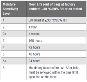
Moisture sensitive device are necessary to be handled and processed following its moisture sensitivity level (MSL) as per industrial standard J-STD-033C. The MSL rated component has to be dry packed with humidity indicator and caution statement – see Fig. 17.
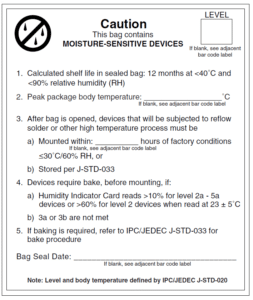
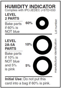
The components shall be processed within an indicated floor life time. Drying and baking before mounting in accordance to the caution instructions are required in case of longer exposure after the bag is opened. MSL classification and floor life time – see fig.18.
Pick & Place
Fast pick and place on large boards may also induce some cracks in chip components such as MLCC capacitors during the component placement. Pressure applied by the Pick and Place nozzle during placement should be carefully monitored and limited. Use of supporting pins to the other PCBs side may limit the board bending and thus reduce mechanical stress to MLCCs. See the following Fig 19.
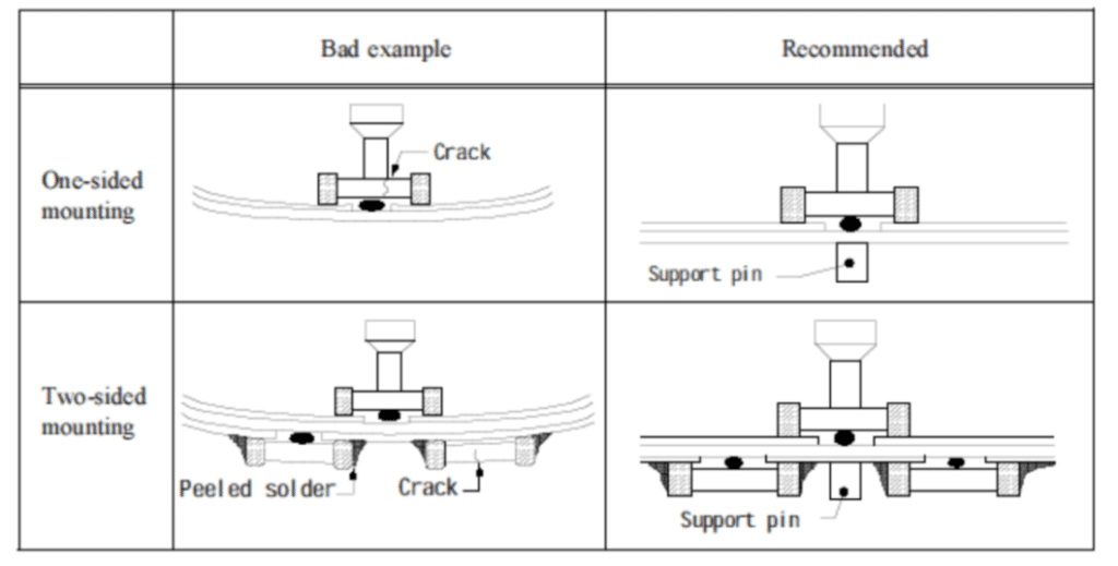
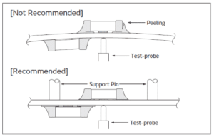
Similar situation as in Fig. 19. can happen during electrical testing of PCBs when test probes are contacting the PCB with push force – see Fig.20. It is recommended to confirm position of the support pin or specific jig, when inspecting the electrical performance of a component after mounting on the printed circuit board. The thrusting force of the test probe can flex the PCB, resulting in cracked chips or open solder joints. The use of support pins on the back side of the PCB can prevent warping or flexing. The support pins shall be positioned as close to the test-probe as possible. Avoid vibration of the board by shock when a test-probe contacts a printed circuit board.
Pick and Place of nearby Components (source: Murata)
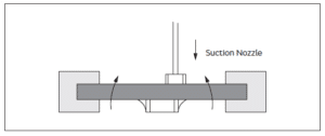
Pick and place of nearby and opposite side components can also cause some flex and PCB vibration. Board deflection stress may damage the back side (bottom side) components if the bottom dead point of the suction nozzle is set too low. After the board is straightened, it is important to set the bottom dead point of the nozzle on the upper surface of the board. Periodical check and adjustment of the bottom dead point is advised as a preventive measure.
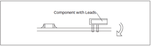
When inserting larger leaded components (transformers, etc.) into boards, the board bending may cause cracks in chip components or cracks in solder joints. The insertion stress can be reduced by appropriate hole size enlargement. It is recommended to fix the board with support pins or a dedicated jig before insertion. Periodically check that there is no difference in the height of each support pin during mass production.
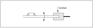
Insertion and removal of sockets and connectors, etc., might be additional cause of board bending. The board shall not warp during insertion and removal of sockets and connectors, etc.
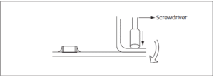
The board may be bent, when tightening screws during attachment of the board to a shield or chassis etc. Mechanical assembly process shall be prepared to minimize board bending, flexing or vibration. Use of torque screwdriver is recommended to prevent over-tightening of the screws. Please note that the board straightness may be impacted by thermal reflow soldering stress. The stress may be applied to the chips by forcibly flattening the board when tightening the screws.