Mounting Techniques Overview
IR reflow soldering
IR infrared “convection” reflow is commonly used in commercial large volume SMD components mounting process. The main differences in reflow soldering processes and oven types lie in heat transfer methods – radiation, conduction, convection and condensation. In fact, all heat transfers are used in modern reflow ovens. The heat is applied from above, below, or all directions dependent on the equipment being used. In classical infrared “radiation” reflow ovens, several ceramic heaters are transferring the heat to the assemblies, moving through the oven on a conveyor belt, by radiation. The limitation was the risk of oxidation and overheating. Nevertheless, the use of fans to help the transfer efficiency by convection minimized highly this issue. Nowadays, the reflow ovens are called “convection ovens” because the heat is mostly transferred by forced air circulation; nitrogen may be used to help wettability in addition.
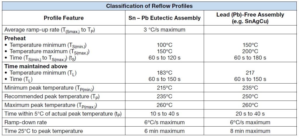
Components are picked from a tape and placed on PCB pads covered by a solder paste. The PCB with components are then placed on a belt that passes through a temperature reflow profile as shown on example figure 2. below. The zones can be split into a four main phases – preheat, peak ramp up, time above liquidus and ramp down time. See classification of reflow profiles as per J-STD-020 in Figure 2. below.
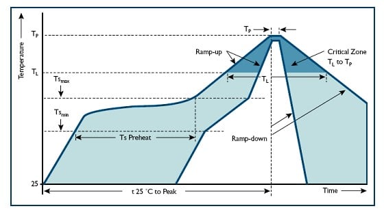
The first preheat phase allow activation of the solder paste flux to clean and de-oxidize the finish of the PCB and components to promote a good wetting. The preheat is also critical to raise the temperature of the PCB and component as uniformly as possible to limit the difference in temperature at solder joint level between different components. The preheat important function from the component perspective is removal of moisture residuals*. The preheat time at temperatures over water boiling temperature is important to provide sufficient time to release moisture even from deep structures and slow moving mechanisms. On the other hand, too long exposure to higher temperature may accelerate some degradation mechanisms and induce some damage to the components.
* Note: Removal of moisture from PCB and component shall be done before assembly following the JEDEC J-STD-033 for industry reference. Despite the moisture removal, some level of residuals may still present inside of deep states inside of components.
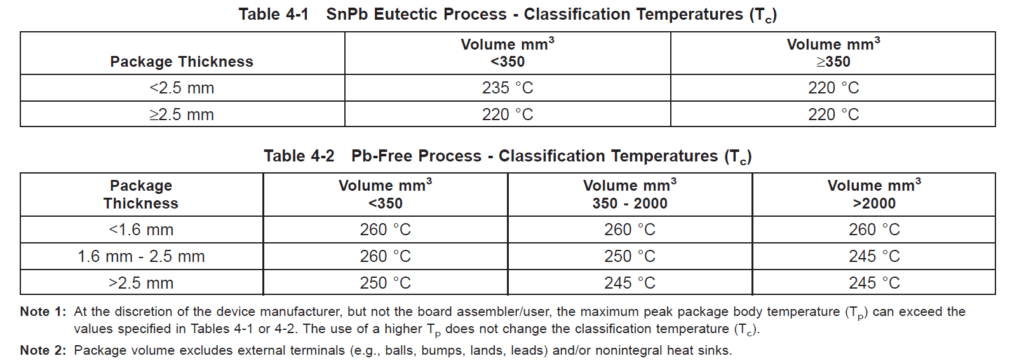
The solder paste is activated during the ramp up phase. The peak temperature, time above a certain temperature (defined by the solder paste melting point) and temperature gradient are the other critical reflow parameters that on one side guarantee a reliable soldering and on the other hand, it may induce some (over)stress to the component. Usually, the peak temperature is set about 20-30°C above the solder paste melting point to provide enough margin for good soldering characteristics in real conditions considering the actual IR reflow oven load (empty vs fully loaded belt), PCB layout, temperature shielding behind larger components, set-up temperature variability (middle oven vs belt edge), set temperature stability etc. The IPC/JEDEC J-STD 020 standard that is followed by majority of industry is classifying peak temperature in relation to the packaging thickness and volume – see Fig. 3 below.
Attention has to be also paid to the number of allowed reflow cycles. J-STD-020 calls for two (two PCB sides) or three reflows (two PCB sides and rework) that components have to survive during the mounting. Nevertheless, this number of cycles may not be achievable by some technologies such as aluminium or film capacitors, thus please always check the manufacturer specification.
The peak temperature gradient, however can be the most critical reflow parameter (even sometimes more critical than peak temperature itself) for many components. Despite the correct preheat zone water removal is present, still some deep moisture residuals can quickly evaporate during the peak temperature ramp up. This may cause a “pop corning” effect with subsequent cracking in the component structure/packaging resulting in imminent parametric, catastrophic short/open circuit or impact to the overall component life time and environmental robustness. The general recommendation is to keep the peak temperature gradient below 2.5°C/s.
The PCB and solder is cooled during ramp down phase. Natural cooling rate is generally recommended; attention has to be paid when forced cooling is used as some components specify the maximum cool down temperature gradient (such as MLCC capacitors).
The PCB and solder is cooled during ramp down phase. Natural cooling rate is generally recommended; attention has to be paid when forced cooling is used as some components specify the maximum cool down temperature gradient (such as MLCC capacitors).
Commonly used solder paste types:
SnPb
- Sn63Pb37 the most common type, melting point 183°C, peak reflow temp ~ 220°C
- Pb content = ROHS Issues
- used in specific applications (defence, space) to avoid tin whisker issues
LeadFree
- most common SnAgCu solder, melting point ~ 217°C, peak reflow temp ~ 245 to 260°C
- JEDEC standards for small components: 260°C, 30sec peak, 3x reflow for large components: 245-255°C
Important Note: Some components such as PET SMD film capacitors are not designed to withstand a lead-free reflow cycle.
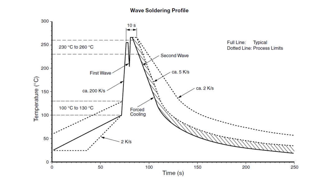
Wave Soldering
The wave soldering process is often used for old designs or/and pin through hole (PTH) components that is more typical for smaller series or simpler designs. The technique is based on one or more hot solder waves used to mount components to the PCB. It is suitable for both through hole components and SMD components glued to the board*.
* note: it can be SMD component specific, sometimes not recommended due to a quick ramp up to liquidus temperature.
In general, the wave soldering is inducing lower thermal stress to the components compare to the IR reflow profile in respect to the total heat exposure time due to the relatively short peak time. The heat may not penetrate in the short time frame such deeply inside the components as in the case of IR reflow. Nevertheless, wave soldering still present some higher load in TCE mismatch and peak temperature gradient with subsequent component damage. A suitable controlled pre-heating is thus recommended to supress the thermal shock impact. (that may be of good help but won’t eliminate the TCE load issue).
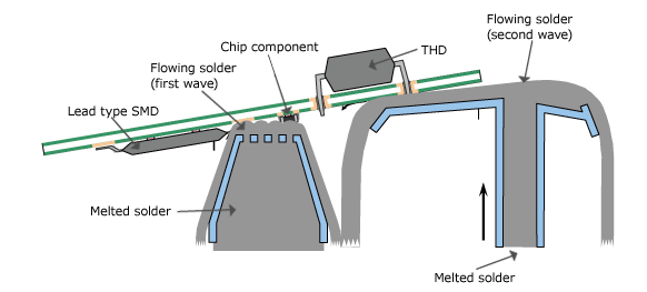

Insufficient pre-heating before the flow soldering or solder dipping may be critical due to the TCE mismatch considerations to sensitive components such as MLCC capacitors. When the thermal stress is exceeding the acceptable construction limit, some external and internal cracking may occur in the ceramic element body.
Vapour Phase Soldering
Vapour phase soldering has been suited more towards lower volume PCB assembly production, mainly due to the cost and extended cycle times, nevertheless step by step it is used more often even at medium volume productions now. Vapour phase well suits high mix, low volume boards and eliminates the need for unique reflow profiles to be created for each product, which can take time. The vapour phase profile, on the other hand, needs to be set up reflecting size of the board and thermal inertia (see the next paragraph).
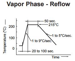
Vapour phase technique is using boiling of an inert heat transfer liquid (e. g. perfluoropolyether PFPE) condensing on the PCBs. The liquid used is chosen with a desired boiling point in mind to suit the solder alloy to be reflowed. Unlike convection reflows, where the PCB travels through heating zones on a conveyor belt, vapour phase ovens are smaller in footprint and the PCB remains fixed in place. The physical height of the PCB is then adjusted so that it sits within, as well as above or just on the surface of, the vapour layer which completes the reflow process. Ref [3]
During the process very little temperature difference (compare to IR reflow) occurs between components of different thermal mass (for example: a large metal heat sink, compared to 0603 chip resistors), which makes it very good for densely populated PCBs and reduces the need for convection reflow peak temperature margin over the solder paste melting point. Thus vapour phase reflow can provide reliable solder joints at lower peak temperature compare to the IR convection reflow.
Components thermal load during vapour phase is usually lower compare to the IR convection reflow due to the lower peak temperature, nevertheless attention has to paid to the peak temperature gradient and time above a certain high temperature not to exceed the component specification. Preheating shall be also applied with vapour phase soldering to reduce thermal issues and improve solder joint quality.
Wire Bonding
Component wire bonding connection is used in some special, lower volume applications such as high temperature or RF applications. Gold plated component termination finish is required in this case. The component is fixed to the board by epoxy glue and connected by ultrasonic gold wire bonding to the components’ top surface.
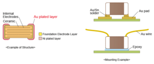
Au-Sn (80/20) brazing alloy at 300 to 320 °C in N2 atmosphere is typically recommended for die bonding conditions of components. Substrate temperature has to match the temperature of the brazing alloy, then the brazing alloy can be placed on the substrate and the component on the alloy. The part shall be hold in position with gently applied load. The operation time shall not exceed 1 minute.
Gold wire 25 micro m (0.001 inch) diameter can be recommended for wire bonding method. The wire bonding joint is performed by thermo-compression and ultrasonic ball bonding. Required stage temperature is within 150 to 200 °C with wedge or capillary weight: 0.2N to 0.5N
The wire bonding method is usually providing a high reliability mount solution with robustness against corrosion/oxidisation and environmental load. Nevertheless, vibration resistance, noise and ESL issues have to be carefully examined.
Adhesive Bonding
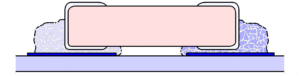
The other alternative component board mounting method is an adhesive bonding. The conductive glue that consists of conductive particles in organic adhesive/binder provide the mechanical and electrical joint between the component and PCB pads. The adhesives can be of “hard” type such as epoxy or “soft” type such as silicon based materials. The adhesives are loaded with usually silver or graphite conductive particles to form isotropic or an-isotropic mount glue.
Low thermal stress and environmental friendly process are the key advantages of adhesive bonding technology. Overall cost, reliability, mechanical strength and electrical conductivity stability under humid conduction are the main concerns associated with this method.
Hand Soldering
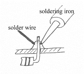
Hand soldering is mostly used for small scale production or re-work operations. In general, hand soldering is not recommended by number of component manufacturers due to the reproducibility and high process variability issues. Requirements of “perfect” solder joint visual standard can sometimes end-up with a nice, shiny solder joint finish, however uncontrolled thermal overstress to the components by not-properly trained operators.
As with wave soldering, the insufficient pre-heating before the soldering may cause some TCE mismatch issues to components such as MLCC capacitors. Insufficient preheating of soldering iron during corrections, or chip contacting the tip of soldering iron may cause heat distortion inside the chip capacitor and cracks may occur in the structure.
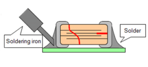
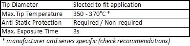
See Fig. 7. for general hand soldering recommendations, nevertheless check and follow the manufacturer recommendations for a specific component type.
Hand soldering at high temperatures can also cause contamination. This contamination & high temperature may cause deterioration of the component overcoat, which could lead to field failures.
Embedding into PCB
Passive components are representing as much as 70% of PCB footprint. The development of a suitable technology whereby integrated passive components is embedded into the PCB body has been one of the key trends in downsizing for more than a decade. The ‘embedding technology’ have been already implemented from pre-production to mass production in number of applications.
Embedding electronic components has been described in publications either as a technique which creates the components directly during PCB manufacturing or as a process where currently existing, specially designed or common electronic components inserted into the inner layers of a board.
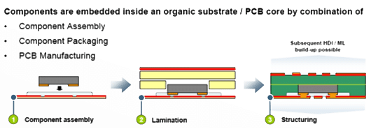
- Component assembly – individual components are placed onto pre-prepared copper foil in a specific position according to the design.
- Component packaging – Step by step treated foils of substrate are placed around and on top of the devices followed by another copper foil. Under pressure and temperature, the sandwich is laminated together to create the core of the new PCB.
- PCB manufacturing – The third step is structuring the copper tracks and layers into required circuits and the construction of the PCB – achieved using existing procedures.
As well as the main advantage, which was already mentioned, namely, the efficient usage of the inner space of the PCBs which leads to a reduction in overall size or an ability to include additional features in the same foot print, passive embedding technology offers other benefits such as improving certain physical and electrical properties.
- Improvement of electrical parameters (for example shorter distance between components)
- Increased reliability (components encapsulated in a protective environment)
- Better resistance to mechanical stress
- Improved thermal properties (better heat sinking)
- Design copy protection.
- Lower thermal shock stress during mounting compare to IR reflow
However, challenges include:
- 3D design skills required
- Supply chain of both, embedding technologies and passives is still limited
- No repair, No rework possible
Component requirements:
Apart from the normal parameters driven by the functionality of passive components, for embedded technology applications, thickness is the most important overall dimension. PCB manufacturers have the ability to embed different thickness of devices depending to number of PCB layers. The standard single PCB layer is typically requiring maximum component thickness 150μm. The component challenges are not only in the maximum component thickness itself, but also it covers tight control of termination thickness variability. Thus use of a specific embedded process ready components is necessary.
Surface finishing may also need some modification to fit better into the construction technology used for the inner structure of the PCB. Standard component technology typically uses a Ni/Sn layer to guarantee a suitable solderability performance for SMD technology. However, for embedding technology processing a copper layer termination surface finish is a better option (depending on assembly technology). There are currently some MLCC embedded capacitors available on the market in maximum thickness of 0.15mm and some specific designs of tantalum capacitor with thickness 0.5/0.6mm suitable for the embedding processing. Source: AVX technical paper.; “Ultrathin Discrete Capacitors for Emerging Embedded Technology”