Soldering, PCB Handling and Rework
Soldering
What is the optimum soldering conditions and solder fillet? The best solder fillet for all SMT applications is one which makes a reliable connection and which best withstands the environmental exposures of the products with minimum degradation. This fillet is difficult to describe quantitatively for all parts. The optimum fillet ranges in height from about 1/3 to 2/3 of the part termination height. This does not mean that all solder joints outside of this range should be repaired. It does mean that this is the target for the process engineer to reach for in his process. As many as possible of the solder fillets on the board should be in this range. [5]
The minimum amount of solder to give a good joint should be used. Excessive solder can lead to damage from the stresses caused by the difference in coefficients of expansion between solder, chip and substrate. If hand soldering cannot be avoided, the preferred technique is the utilization of hot air soldering tools.
In general, most of capacitors and resistors are suitable for all vapour phase wave and reflow soldering systems, nevertheless please check the manufacturer’s relevant datasheets and guidelines. Common temperature profiles and specifications – see the industry standards Chapter 2.
Some limitation exists mainly for film capacitors regarding the use of convection profile and maximum peak temperature. Temperature profiles are specified in the CECC 00802 standard. Temperature peak limits for most common film dielectrics are:
- E.T. = 215°C (20 s at 40 s)
- E.N. = 230 C (20 s at 40 s).
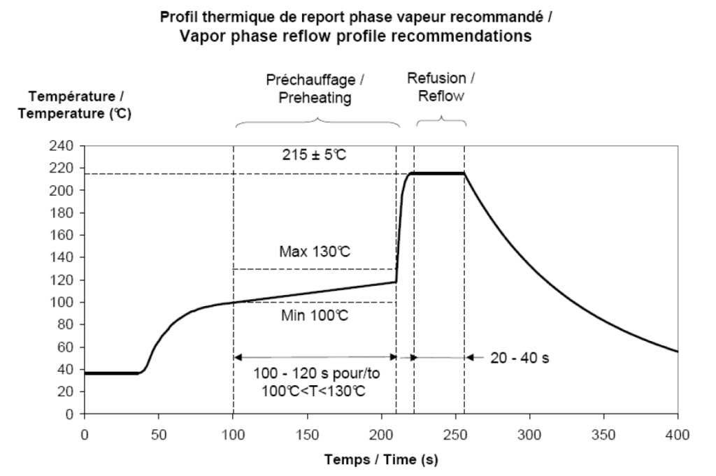
Important note: PET film capacitors are not designed to withstand a lead-free reflow cycle, use of vapour phase mounting can be recommended. See Fig.21 below for PET SMT film capacitors vapour phase profile recommendation.
Flux
Use of mildly activated rosin fluxes in the solder are preferred. More “aggressive” flux is improving the solder wetting and solder joint strength, on the other hand it is increasing oxidisation and require thorough cleaning process to remove all flux residual. Most manufacturers do not recommend use of highly activated fluxes due to this reason. Water soluble fluxes are not recommended for some resistor technologies using a thin resistive film. Water soluble fluxes are very aggressive in stripping off oxides and if you do not completely clean the residue off, then it can continue to eat away at the base metal. Please follow the manufacturers specification for details.
Preheat
It is important to avoid the possibility of thermal shock during soldering and carefully controlled preheat is therefore required. The rate of preheat should not exceed 4°C/second and a target figure 2°C/second is recommended. Although an 80°C to 120°C temperature differential between preheating and peak temperature is preferred, recent developments allow a temperature differential between the component surface and the soldering temperature of 150°C (Maximum) for capacitors of 1210 size and below with a maximum thickness of 1.25mm. The user is cautioned that the risk of thermal shock increases as chip size or temperature differential increases.
Cooling
Natural cooling in air is preferred, as this minimizes stresses within the soldered joint. When forced air cooling is used, cooling rate should not exceed 4°C/second. Quenching is not recommended but if used, maximum temperature differentials should be observed according to the preheat conditions above.
Solder Joint Quality
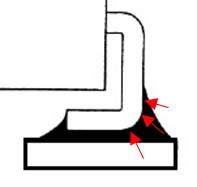
Soldering quality shall be regularly examined in order to access the mounting process correct set-up. The solder joint has to provide sufficient mechanical strength and electrical features. One of the critical factor for SMD “J” type is a full coverage of the termination bend area with a sufficient solder wetting that ensures proper solder joint mechanical strength.
Reflow conditions (tinning thickness on boards, amount of soldering paste deposited, reflow soldering process, etc.) should allow, after reflow, a solder filet on the SMD “J” lead components look as shown on Fig.22. Solder height should cover the connection bend by about 0.5 mm and finish on the vertical side of the connection. Good wetting ability of the solder fillet can be assess with the wetting angle.

Cleaning
Flux residues may be hygroscopic or acidic and must be removed. Passive components are usually acceptable for use with all of the solvents described in the specifications MIL-STD-202 and EIA-RS-198. Alcohol based solvents are acceptable and properly controlled water cleaning systems are also acceptable.
Care should be taken to ensure that the components are thoroughly cleaned of flux residues especially the space beneath the component. Such residues may otherwise become conductive and effectively offer a low resistance bypass to the capacitor.
Excessive ultrasonic power or direct vibration transfer to a printed wiring board may generate a resonant vibration in the board. This may cause a crack in sensitive components (such as MLCC capacitor) or its solder joints to the board and degradation in the terminal strength of the capacitor. In order to avoid this, the following cleaning conditions are recommended:
Power: ≦20 W/L
Frequency: ≦40 kHz
Duration: ≦5 min
NOTE: The details is referred to JEITA ET-7405, and the bath size is 250 mm X 200 mm X 180mm(depth)
The most commonly recommended ultrasonic frequency is 40 kHz. It is considered the “universal frequency” because it is generally safe for use in most applications and will produce the most intense cavitation energies to remove the most common types of contaminants (oil, grease, metal chips) from the widest range of substrates. Lower frequencies such as 20 or 25 kHz produce larger cavitation bubbles which are more aggressive when they implode. Higher frequencies (68-250 kHz) will produce smaller cavitation bubbles with less intense energies, but more of them. [19]
Before starting your production process, test your cleaning equipment/process to insure it does not degrade the components. Exposure to harsh ultrasonic cleaning after mounting; shower washing; covering with masking tapes may cause component termination(s) to peel. Caution should be taken when cleaning is performed.
Post Solder Handling
Once SMD components are soldered to the board, any bending or flexure of the PCB applies stresses to the soldered joints of the components. For leaded devices, the stresses are absorbed by the compliancy of the metal leads and generally don’t result in problems unless the stress is large enough to overcome the stress relief provided by the lead.
Ceramic capacitors are more susceptible to such stress because they don’t have compliant leads and are brittle in nature. The most frequent failure mode is low DC resistance or short circuit. The second failure mode is significant loss of capacitance due to severing of contact between sets of the internal electrodes. [8]
Common Causes of Mechanical Cracking
Cracks caused by mechanical flexure are very easily identified and generally take one of the following two general forms:

Mechanical cracks are often hidden underneath the termination and are difficult to see externally. However, if one end termination falls off during the removal process from PCB, this is one indication that the cause of failure was excessive mechanical stress due to board warping.
If a board mounted with capacitors is held with one hand, the board may bend. Firmly hold the edges of the board with both hands when handling. If a board mounted with capacitors is dropped, cracks may occur in the capacitors. Do not use dropped boards, as there is a possibility that the quality of the capacitors may be impaired.
The most common source for mechanical stress is board depenalization equipment, such as manual break apart, cutters and shear presses. Improperly aligned or dull cutters may cause torqueing of the PCB resulting in flex stresses being transmitted to components near the board edge.
Another common source of flexural stress is contact during parametric testing when test points are probed. If the PCB is allowed to flex during the test cycle, nearby ceramic capacitors may be broken.
A third common source is board to board connections at vertical connectors where cables or other PCBs are connected to the PCB. If the board is not supported during the plug/unplug cycle, it may flex and cause damage to nearby components. Special care should also be taken when handling large (>6″ on a side) PCBs since they more easily flex or warp than smaller boards.

PCB Coating, Potting and Molding
In general, coating, potting, molding or sealing of the assembled PCB can be recommended in order to supress moisture, oxidisation and other environmental impacts. Nevertheless, the process has to follow the manufacturer specifications as it can affect the mounted components parametric values (such as capacitance, resistance, ESR, DCL etc.) due to a thermal stress effect, TCE expansion or shrinkage of the component overcoat/moulding package etc.
PCB Cut and Cropping
Check the cropping method suitability for the printed circuit board in advance. Printed circuit board cropping shall be carried out by using a jig or an apparatus (disc separator, router type separator, etc.) to prevent the mechanical stress that can occur to the board. The board separation recommendation from Murata – see Fig 25.
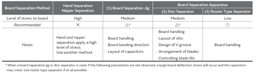
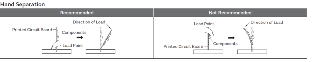
In case of hand separation of single side board is used, stress on the component mounting position can be minimized by holding the portion close to the jig, and bend in the direction towards the side where the components are mounted. Not recommended example: The risk of cracks may increase due to large stress being applied to the component mounting position, if the portion away from the jig is held and bent in the direction opposite the side, where the components are mounted –see Fig.25.
In case of double side board, where the above Fig.26 method cannot be used, consider introducing a router type separator. If it is difficult to introduce a router type separator, mount the components parallel to the board separation surface. When mounting components near the board separation point, add slits in the separation position near the component and keep the mounting position of the components away from the board separation point – see Fig.27.
To avoid many of the handling problems, manufacturers are recommending that MLCCs be located at least 5mm away from nearest edge of board. However, when this is not possible, the panel be routed along the cut line, adjacent to where the MLCC is located.

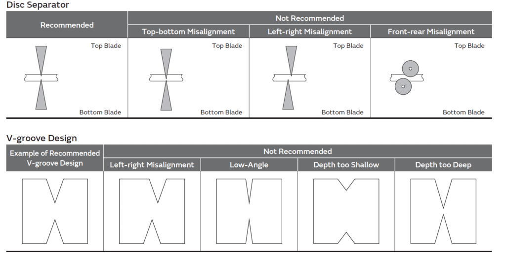
Board deflection stress component cracks may also result in misaligned disc or V groove separation machines set-up. See Fig. 28. IF V groove is too deep, it is possible to brake when you handle and carry it. Carefully design depth of the V groove with consideration about strength of material of the printed circuit board.
PCB Storage
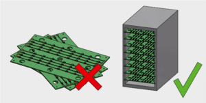
By stacking the PCB boards, sensitive components might be deformed or delaminated due to the mechanical stress. Use a proper and suitable rack to keep the finished and assembled PCB boards correctly – see Fig 29.
The PCB has to be stored in “environmental standard” conditions and such conditions has to be also maintained during transportation and manipulation. Extra care has to be paid to sea and air transportation or “unattended on the hold short term storage” at direct sunshine etc.
Rework
When performing manual repair or reworking, it is necessary to pay attention to the following two issues, particularly because of temperature change and residual stress. It is also necessary to consider thermal capacity of the PCB in order to optimise the rework procedures.
- In order to prevent damage (cracks) to the component caused by localized rapid heating and heat shock: baking of PCB, component preheat or other measures to reduce heat shock to the parts shall be applied.
- The board temperature is lower than that used for reflow soldering, so a difference in residual stress occurs during cooling, and the mechanical strength (resistance to board bending) tends to decrease. In order to increase the strength, it is necessary to maintain a high board temperature during soldering.
Solder Iron Rework
In order to reduce damage to the capacitor, be sure to preheat the capacitor and the mounting board. Preheat to the temperature range depending to MLCC capacitor case size is shown as example in Fig. 30.

A hot plate, hot air type preheater, etc. can be used for preheating. After soldering, do not allow the component/PCB to cool down rapidly. Perform the corrections with a soldering iron as quickly as possible. If the soldering iron is applied too long, there is a possibility of causing solder leaching on the terminal electrodes, which will cause deterioration of the adhesive strength and other problems.
Optimum solder amount when re-working with a soldering iron is needed. If the solder amount is excessive, the risk of cracking is higher during board bending or any other stressful condition. Too little solder amount results in a lack of adhesive strength on the outer electrode termination, which may result in chips breaking loose from the PCB. A soldering iron with a tip of ø3mm or smaller should be used. It is also necessary to keep the soldering iron from touching the components during the re-work. Solder wire with ø0.5mm or smaller is required for soldering. [11]
Spot Heater Rework
Compared to local heating with a soldering iron, hot air heating by a spot heater heats the overall component and board, therefore, it tends to lessen the thermal shock. In the case of a high density mounted board, a spot heater can also prevent concerns of the soldering iron making direct contact with the component.
If the distance from the hot air outlet of the spot heater to the component is too close, cracks may occur due to thermal shock. To prevent this problem, follow the conditions shown in Fig. 31 below.
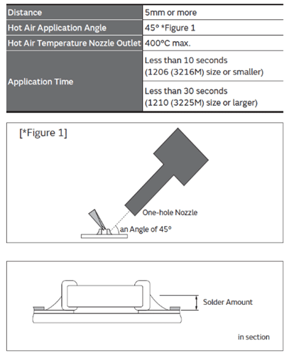
In order to create an appropriate solder fillet shape, it is recommended that hot air be applied at the angle shown in Figure 31.
Thermal shock is common in MLCCs that are manually attached or reworked with a soldering iron. Manufacturers are strongly recommending that any reworking of MLCCs be done with hot air reflow rather than soldering irons. It is practically impossible to cause any thermal shock in ceramic capacitors when using hot air reflow. However direct contact by the soldering iron tip often causes thermal cracks that may fail at a later date. If rework by soldering iron is absolutely necessary, it is recommended that the wattage of the iron be less than 30 watts and the tip temperature be <300ºC. Rework should be performed by applying the solder iron tip to the pad and not directly contacting any part of the ceramic capacitor.

Component Storage
In general, resistors and capacitors good solderability is maintained for at least twelve months, provided the components are stored in their “as received” undamaged packaging (important especially for MSL sensitive parts delivered in dry packs) at typical standard conditions:
- Temperature: -10°C to +50°C
- Humidity: 75% RH maximum (or 45-85% RH depending on component)
- Atmospheric pressure: 860 mbar ~ 1060mbar
Avoid the storage in the following environment:
- storage in places full of corrosive gasses such as sea breeze, Cl2, H2S, NH3, SO2, and NO2.
- storage in places exposed to direct sunlight
- storage in places outside the temperature range of 5deg to 35deg and humidity range of 45% to 85%RH.
- Storage over a package expiry date
Depending on component type, the storage can be prolonged to 2 years or longer, or re-lifed if the product specification allows it. Please follow manufacturer instruction for the specific product.
Re-Life
Some components allow re-lifing of components to extend its shelf life. Please follow the manufacturing instructions, example of such instruction can be as follows for film and MICA capacitors (source: Exxelia):
- From 0 to 12 months: no instructions, standard shelf life
- From 12 to 18 months: dried in a ventilated chamber, conditions = 24 hours at 100°C for film technology and 24 hours at 125°C for mica technology.
- From 18 months to 2 years: dried in a ventilated chamber, conditions = 48 hours at 100°C for film technology, 48 hours at 125°C for mica technology. When removed from storage the capacitors should be used within 3months. During this period extreme care should be taken in handling all high voltage components. If the capacitors are not used within the 3 months period the following procedure should be followed: cleaned, dried in a ventilated chamber, conditions = 24 hours at 100°C for film technology, 24 hours at 125°C for mica capacitors.
Note: the storage time is the time between delivery and the date of unpacking from the original packaging
References:
[5] Kemet guideline “Wave Solder Process for Surface Mount Applications”; www.kemet.com
[8] AVX catalogue “AVX MLCC surface mount capacitor catalogue“; www.avx.com
[11] Murata “Caution notice for automotive“; www.murata.com
[19] Product Finishing article online “Ultrasonic Cleaning Systems Deliver Results and Efficiency“; www.pfonline.com