
Filters and RF Inductors
In this article about filters and RF inductors we shall deal with wider filter introduction that also includes capacitors and resistors and focus then on EMI and RF inductors.
The article is split into following chapters:
- Filters Basic Concepts
- Filter Construction
- LTCC Components and RF inductors
Filters Basic Concepts
Filters that contains one or more capacitor elements with paper, plastic film or ceramic dielectric combined with one or more inductive elements in the form of ferrites or chokes are called LC filters. Ceramic capacitors used are of feed-through type, where one terminal consist of the casing that is soldered or screwed to the chassis. Or there are SMD variants.
It should also be mentioned that there are RC filters where an metallized paper (MP) capacitor is combined with a series resistance. Often the resistor element consist of a metallization alloy with higher resistivity. RC filters are mainly used for arc suppression purposes.
Some abbreviations

- RF = radio frequency = frequencies where radiation starts to appear
- RFI = radio frequency interference = induced radio frequent interference signals
- EMI = electromagnetic interference
- I.L. = Insertion Loss
- A = Attenuation
Measurements and Concepts
A filter should eliminate interference signals but transmit effective capacity and signal currents. Normally the interference signals are located in the RF range and the true signal/power currents in the low frequency range. Thus the filter should transmit low frequency signals and suppress those of higher frequencies. We call this the low-pass filter. There are, however, also other filter types as shown in Figure 1.
The common low pass filter can be described in Figure 2.
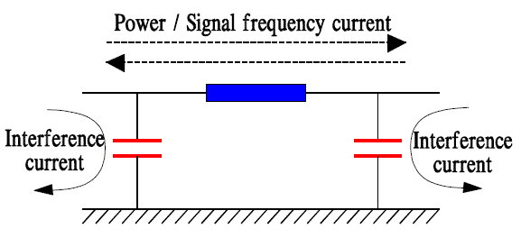
The figure shows how the interference currents are blocked by an inductor and lead away to earth via capacitors. Thus following filter concepts mainly applies to interference signals and interference frequencies.
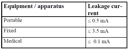
There is, however, an important exception. Filters connected between phase and earth in the mains contain those Y safety capacitors. Through them will flow a weak current at the net frequency. It is called leakage current and has to be limited to certain values. The following table 1. shows some generally accepted limits.
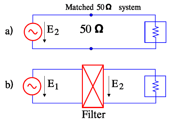
Attenuation
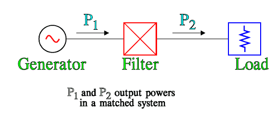
The attenuation, A, is expressed in dB and is determined in a matched system, i.e., where generator, line, filter and load have the same impedance, as a rule 50Ω.
In the system there is no reflection either from the filter or from the load. Then the attenuation A is defined as in eq.[1]:

Often the minus sign is left out when we speak of attenuation.
Insertion loss, I.L.
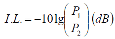
It is very seldom that a filter is matched to the system. Then, in a strict sense of specification, we don’t speak of attenuation but of insertion loss, abbreviated I.L.
P1 represents the output power without a filter and P2 the output power from an inserted filter. The difference includes both specified attenuation and return losses. Less formally the expression attenuation is used as a measure of the signal reduction of the filter, irrespective of circuit conditions.
MIL-STD-220 defines I.L. as:
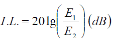
where the voltages before and after filter insertion are illustrated
in right Figure 4.
If we apply a load in the circuit that differs from the line impedance, the I. L. will be changed. The attenuation of the filter in its turn depends among other things on the DC current. Maximum DC current – full load operation – impairs inductor inductance. The attenuation decreases. Note therefore in catalogues and specifications if the I.L. concerns No load or Full load values.
If the attenuation characteristics are to be correctly established it is important that the generator side is effectively shielded from the receiver side. Moreover it is necessary to use shielded cables, correct connectors and test fixtures supplied with shielding walls.
The manufacturer’s data over I.L. is a guidance. In the practical circuit, however, the attenuation generally is poorer.
Filter Types and Their Mounting
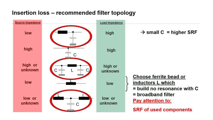
The LC filters are built up by their elements in certain basic configurations. In the following sequence of figures it is shown which basic style that has to be used in different impedance conditions in order to reduce the mismatch.
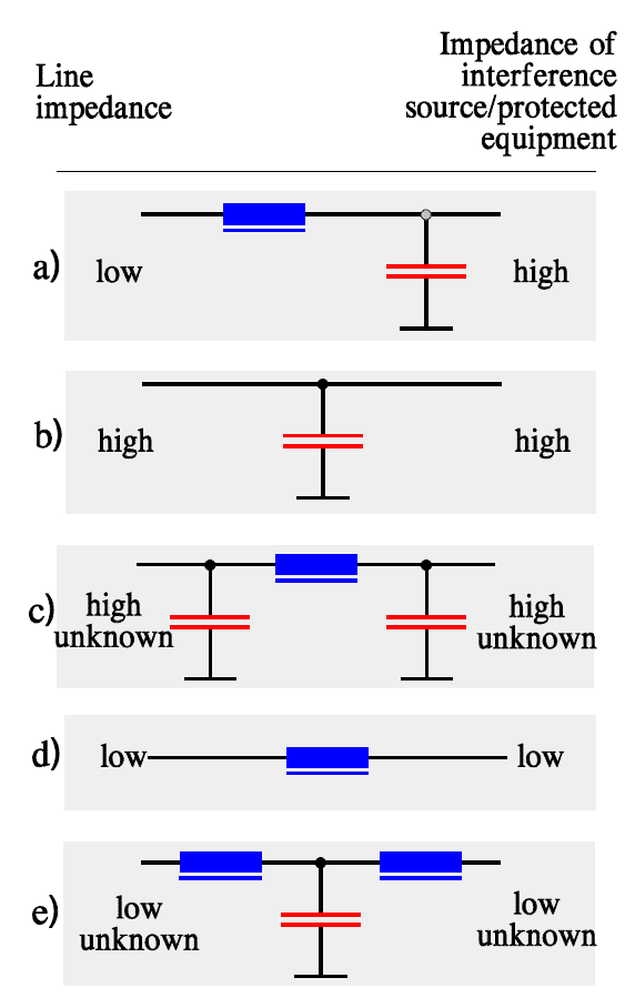
Filter types:
a) = L
b) = C
c) = π
e) = T
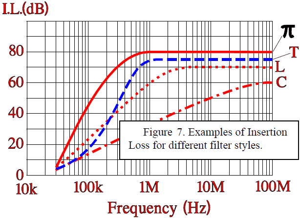
Theoretically, these filter styles have insertion
losses as shown in Figure 6. below:
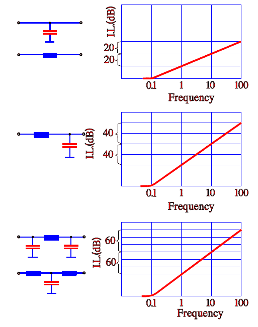
The next Figure 7. shows some examples of how the same basic elements added together in different configurations influence the attenuation in practical filters. All attenuation curves usually start leveling out at approximately 70 – 80 dB. Further attenuation is prevented by inductance and series resistance in the capacitor elements and parasitic capacitance and resistances in the inductor elements. A general recommended filter topology depending to source and load impedance requirements is shown in Figure 8.
Filter Construction
HF / π / EMI / RFI filters
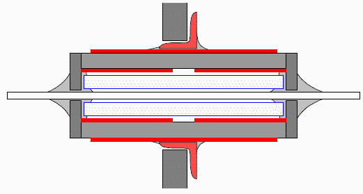
This type of LC filter consists in its most simple design of elements arranged as in Figure 5a or 5b. The most common types look like the one in Figure 5c. They have a feed-through design, i. e., the capacitor elements are connected direct to earth when the plated outside of the filters is soldered to the housing wall. A typical design of an EMI filter of the p type is shown in next Figure 9.
Usually the π filters are supplied with a collar that is soldered to the silvered surface (Figure 10.).

Note! If the collar in the filter in Figure 10. is soldered with a high temperature solder, check carefully that there is no unintentional solder on the top side of the collar. This would increases the outer diameter of the bushing so it will not fit in the intended hole.
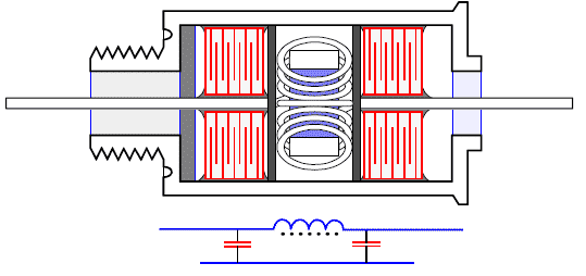
EMI filters often are sealed in metal housings that are encapsulated hermetically (Figure 11.) or by epoxy encapsulation. The capacitor elements consist of concentric chips, so called discoidals, that are soldered to the metal housing. The cases are supplied with a threaded part. More powerful filters often are supplied with a toroidal choke. They usually are built in π, L or T configurations. The stated capacitance value many times is a minimum
value, sometimes abbreviated as GMV, i.e., guaranteed min value, because it is the specified minimum attenuation that is of interest.
Failure modes
The discoidal design should be preferred to the ceramic tube design. The thin ceramic tube is brittle and has to be protected against mechanical damage and temperature gradients at the soldering. A treacherous source of errors may appear at the soldering moment. If, for example, in Figure
9. or 10. the right part of the lead-through wire is soldered and the solder heat happens to melt the seal solder around the filter inlet, the filter will be anchored in the lead-through wire only to its left solder joint.
If we then touch the right part of the lead-through wire – and this will happen during the soldering – we get a bending moment that is transferred to the ceramic tube in its fixed position to the wall. Usually it cracks. If we run the risk of melting internal solder joints we should specify high temperature solder for internal construction. The melting point usually is in the vicinity of 300 °C.
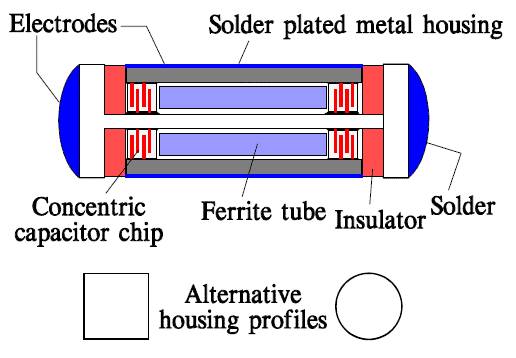
For hermetic EMI filters short-circuiting in a capacitor element is the most common. Often it is a matter of cracks in the ceramic that have cleared the way for migration of electrode metals or flux contaminants and a subsequent breakdown. Open circuit may occur and depends usually on poor internal solder joints.
SMD designs
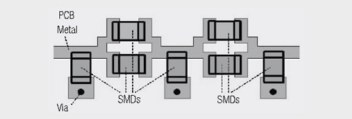
Figure 12. shows a construction sketch of a section through a π filter chip.
Simpler variants of π filter chips have the same buildup as the filter in Figure 8. Other designs utilize a multi-layer technique for both the capacitor and the ferrite elements. The most simple design has a T-circuit configuration with two ferrites and one capacitor connected to the ground terminal.
Integrated EMI filters
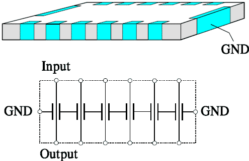
If we by means of multilayer technology build a number of ceramic capacitor elements into a ceramic block in a planar array construction we may save a considerable board space (see more in next LTCC filters chapter). Moreover, we will increase the electrical filtering capability due to reduced inductance in shorter internal conductors. This type of capacitor arrays is preferably used in EMI suppression applications. An example of such a design is shown in Figure 13.
Filters in connectors are constructed in the same way but in shape of circular discs with discoidals arranged around the pin feedthroughs. Electrical connections are through via and edge terminations.
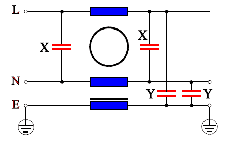
Another EMI filter, also consisting of integrated ceramic capacitors, is built of a matched and balanced pair of Y capacitors (line to ground) together with an X capacitor (between the lines) connected to a four-terminal device4 as shown in Figure 14. The device is called X2Y.
A principle sketch of the construction looks like as shown in Figure 15.
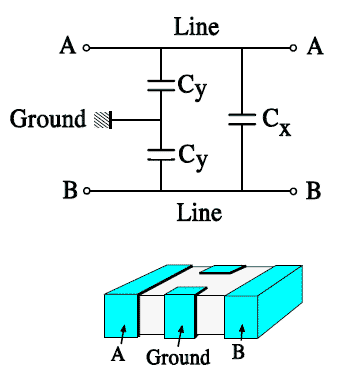
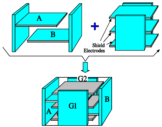
X and Y capacitors in an X2Y device reflect the patented design shown in Figure 15. These EMI filters are mostly used in lower voltage applications but larger sized X2Y devices can be designed also for mains applications where they for safety reasons require test voltages far above 1 kV.
The EMI filter X2Y has many advantages. The inserted ground planes reduce the current loop in comparison to standard MLCCs thus decreasing the inductance of the device. A further inductance reduction is achieved by the opposite current direction in opposed electrodes that is possible by the inserted ground planes. All these measures mean more effective filtering at higher frequencies.
In our Figure 15. above only two electrodes and three ground planes are shown. In practice the number of electrodes and intervened dielectric layers may be much greater, depending on the intended capacitance. The EMI filter X2Y is produced in sizes 0603 to 1812. Rated voltages for the Y capacitor elements in NP0 dielectric are 100V, in X7R dielectric 10 to 100V and in Y5V dielectric 16V. Rated voltages for X capacitors are correspondingly greater. The capacitance ranges from 10 pF in NP0 to 10mF in Y5V dielectric. Apart from the above mentioned advantages the design offers a size reduction in comparison to discrete MLCCs by integration of three capacitors in one device.
Power Line Filters
These filters often are supplied with toroidal chokes and usually have considerably more elements than in the simple π filter.
LTCC Components and RF Inductors
The use of LTCC (Low Temperature Co-fired Ceramic) material is gaining importance in applications in the field of communications. This is a multi-layer process used for the production of sophisticated HF components with good performance characteristics. The ceramic-based LTCC technology is an inexpensive substrate technology with which up to 50 layers are stacked on top of each other. The silver or gold conductor tracks are impressed on the “green” ceramic foil once the holes for the through contacts have been laser or mechanically generated. The various layers are then collected together and are pressed in a pressure chamber. Following lamination, the stack is sintered in a furnace, i.e. burned together at around +850 °C in process furnaces.
LTCC can be used to produce multi-layer modules in which cavities, Rs, Ls and Cs are integrated. Good thermal conductivity and a low TCE (Temperature Coefficient of Expansion) are achieved. The components are hermetically sealed, i.e. are stable against mechanical and thermal stress. The dielectric properties (R, tand, the thickness) can be controlled very effectively.


The main advantage of this technology is the high degree of miniaturisation and the ever-lower space requirement associated with it. This is illustrated by the following simple example. Rather than discreetly constructing a low-pass filter, there is the option of integrating the inductance and capacitance, e.g. as package type 0603. The integration is an important aspect in the field of RF applications.
Low-Pass Filter
HF components based on LTCC technology are designed for use in various frequency bands from around 900 MHz to 6 GHz. Application areas for these components are, for example, Wireless LAN, Bluetooth®, HomeRF, GPS, PCS, GSM, DECT and PHS.
The high precision LTCC technology gives rise to low-loss RF components with reproducible, guaranteed properties and a low space requirement.
LPF low-pass filters for diverse applications are produced in the package types 0603 to 0805. The limit frequencies of these compact low-pass filters range form 900 MHz to 5.5 GHz. The insertion loss of the low-pass filter in the admission range is very low. The low-pass filters show comparably high attenuation in the blocked range.
Band-Pass Filter BPF
The smallest band-pass filter package type is 0805. A high level of attenuation is achieved over a very wide blocking range. The insertion loss in the admittance range is very low at approx. 2 dB, however somewhat higher than the insertion loss of low-pass filters.
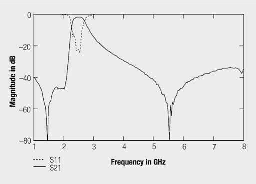
The example of the band-pass filter for Bluetooth® serves to illustrate where attention should be paid in the selection of components. (Figure 20.)
To effectively suppress frequencies in the mobile phone range, the attenuation in the range from 900 MHz (GSM900) to 2.1 GHz should be as high as possible. The attenuation in the WLAN/HyperLAN range should also be high. For this reason, specific poles have been placed at these frequencies for the above filter.
Balun BAL
Symmetry transformers (baluns) with low insertion loss, as well as low amplitude and phase differences, can be achieved in LTCC technology. The asymmetrical (unbalanced) impedance is 50 Ω, the symmetrical (balanced) impedance can be 50 Ω, 100 Ω or 200 Ω. Two types of baluns are distinguished: LC type and Marchand type. In the case of the latter, no DC bias may be applied. It is recommended to connect a capacitor to ground in front of the pin where the DC voltage is input. Information on external circuitry and layout recommendations may be found in manufacturers’ datasheets.
Balun with Integrated Band-Pass Filter
A band-pass filter and a balun can be integrated into a component to reduce the space requirement. Besides the high attenuation in the blocking range, low insertion loss is also achieved. The admission range of this component lies typically in the frequency range 2400–2500 MHz. Numerous other components, such as diplexers, couplers and couplers with integrated low-pass filter or dual-band baluns, are available in this multi-layer technology on the market.
Multilayer MCA
The MCA chip antennas based on LTCC technology stand out by virtue of their compact constructions and low weight and are suitable for applications in the fields of GPS, Bluetooth, 802.11b+g, UNII and 802.11a as well as for 868–960 MHz, also available as dual & triple band. In relation to their size, the antennas offer a large bandwidth and are easy to match. The input impedance is 50 Ω. The typical gain, depending on the antenna type, is around 1dBi. The radiation properties of the antennas can be termed plane omnidirectional. Alignment charts are presented in manufacturers’ datasheets.
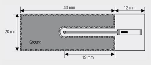
The electrical parameters of the chip antennas are measured with test boards as shown in example Figure 21. Many factors, e.g. the board type (dielectric constant) and the layout, affect the electrical properties of a chip antenna. The component values for the matching network shown in the datasheet cannot be assumed for this reason. These values only apply for the test boards used; they may however be used as starting values for determining the matching network in the application. The return loss can be significantly improved by matching the antenna.
To achieve the performance shown in the datasheet, it is important to ensure sufficient separation between the antenna and the ground plane. The antenna is preferably placed at a corner point of the board to avoid that the antenna is completely surrounded by a ground plane. Deviations from the suggested layout instructions can lead to changes in the alignment characteristics and input impedance. In general, care must be taken that the separation between the long side of the antenna and the ground plane is at least 5 mm. The separation between the antenna surface and the housing must be at least 1 mm.
The microstrip feed lead can be considered as part of the antenna system. It is recommended to connect the ground plane surrounding the input lead on the edges to the lower ground with through contacts. This serves to minimise the electric field on the edges and hence its influence on the antenna.
The efficiency η is the ratio between the radiant power and the input power. The efficiencies of the chip antennas derived from numerical calculation are presented in the following table. This includes antennas operating in the frequency range 2400–2500MHz. Essential differences are the antenna dimensions and the gain. The standing wave ratio is a maximum of 2 for all antennas within the bandwidth.
RF Inductors
Air Coil KI; RFH; RFI
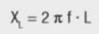
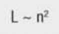
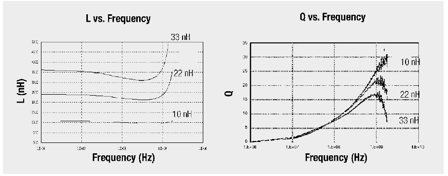
The classic inductor is a configuration of one or more wire windings on a magnetically non-conducting coil former. In contrast to coils with magnetic coil formers or cores, this component‘s advantage is in its current independent inductance and the fact that it shows no saturation effect. Further very important advantages are the linear impedance over a wide frequency range, eq. [4] and a very high quality factor Q (typ. 50–100). The relationship for an inductance L and the winding turns n can be then approximated as shown in eq. [5].
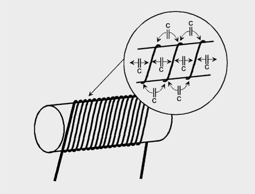
The air coil has a parasitic capacitance dependent on winding diameter, wire thickness as well as layer and winding structure, which mainly exists between neighboring windings (Figure 22.), but for SMD components also occurs between both the connection pads.
The self-resonant frequency, above which the component shows capacitive characteristics, results from the inductance and the parasitic capacitance.
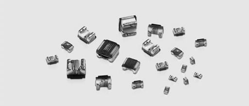
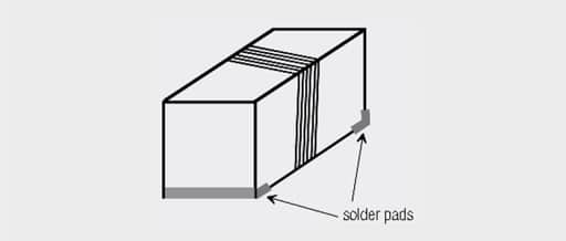
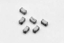
The series of KI ceramic SMD inductors are examples of air coils (Figure 23.).
The solder pads on the coil former are designed to be very small (Figure 24.), in order that the inductors achieve a high self-resonant frequency. Self-resonant frequencies of well above 10 GHz are thus attained.
If higher current carrying capacities are required, the components can be wound on ceramic or ferrite cores depending on the inductance value.
RF Multilayer Ceramic Inductor
The construction of an SMD inductor (Figure 25.) differs from that of a conventional air coil in that the “coil” is printed on a ceramic substrate. This presents the following advantages:
- Very low inductances achievable
- Very low parasitic capacitance and therefore high resonant frequency
- Relatively high current carrying capacity of typ. 300 mA
The specifications of 0201 multilayer ceramic SMD inductor is shown in Figure 26.
The preferred field of application of these components lies in the high-frequency range, in filter circuits and oscillator circuits.