Transformer Calculation, Losses and Applications
How to calculate transformator, which losses and parasitic parameters are there in the transformer and how can they be measured and subsequently represented in a simulation model? What are applications design specifics?
Have a look into details in the following chapters of the article:
- Transformer Losses, Parasitic Parameters and Equivalent Circuit
- Transformer Application Requirements – Return Loss Effect
- LAN, Telecom and Power Transformers
Transformer Losses, Parasitic Parameters and Equivalent Circuit
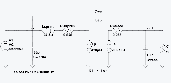
“Ideal” transformer models are usually used to make it as easy as possible for the developer and to reduce the computation time in LTspice. Only the inductance values for the primary and secondary are required here, as well as the coupling factor K (here in statement K1 Lp LS set to 1 = ideal).

The simulation results are far closer to practice if the coupling factor is already taken into consideration [1], because transformers have stray inductance of 2% ~ 8% depending on the construction.
We use the following equivalent circuit for further consideration and to determine the parasitic elements:
- Cww: winding – winding coupling capacitance
- Cwprim: primary-side winding capacitance
- Cwsec: secondary-side winding capacitance
- Lsprim: total stray inductance (primary + transferred secondary stray inductance)
- RCuprim: primary Cu resistance
- RCusec: secondary Cu resistance
- Lp: primary inductance
- Ls: secondary inductance
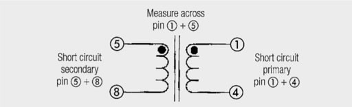
Measuring the Primary and Secondary Inductance
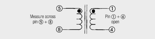
To measure the primary and secondary inductance, the respective winding not measured must remain open.
ratio n
The turns ratio n can be calculated as follows
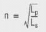
For Lp = 939 µH and Ls = 26.87 uH in Figure 1. example, the calculated turns ratio is 5.91.
Total Stray Inductance
Primary stray inductance and transferred secondary inductance can be measured by short-circuiting the secondary winding (pin 5/8) and measuring between pins 1/4.

Please note:
The stray inductance is as well in series with the transmission path . The stray inductance describes that part of the magnetic field, which is not enclosed from the respectively other winding and therefore contributes not to the coupling . The stray inductance results simply from the mechanical arrangement of the windings against each other . A decrease of the stray inductance comes along with the increase of the coupling capacitance . The total stray inductance (primary inductance + transferred secondary stray inductance) is measured by measuring at short circuited secondary winding (Please note: To not distort the measurement result a low impedance short circuit is necessary) .
Many applications demand as small a stray inductance as possible. It can be minimized using various winding techniques. The windings should be as wide as possible. A sandwich construction also helps, as in the case of the proximity effect. However, these techniques increase the coupling capacitance between the primary and secondary sides.
DC current winding resistances
RCuprim and RCusec between pins 5/8 and 1/4 respectively can be measured with an ohmmeter. Example RCuprim: 265 mΩ and RCusec: 858 mΩ
Coupling capacitance
Additional parasitic parameters include the coupling capacitance (capacitance between the primary and secondary sides) and the winding capacitance (capacitance between the turns of a winding). The influence of coupling capacitance on the circuit can be reduced by shielding windings between the primary and secondary sides. However, minimization of the coupling capacitance by winding in several sections or by inserting thick insulation between the primary and secondary side directly causes an increase in stray inductance. The coupling capacitance can be measured directly. The winding capacitance is measured indirectly via the resonance between the main inductance and the capacitance. An LCR bridge is used to measure from winding to winding, in this case between pins 1/5. For measurement reasons both windings should be separately short-circuited so the measurement result is not distorted.
Winding capacitances
The winding capacitances can only be determined indirectly from the resonances with the main inductance (Lprim/Lsec). The impedance with the secondary side “open” is measured with an impedance analyzer. The winding capacitance of the primary side is then calculated from the resonant frequency.

- Lprim main inductance
- Cw winding capacitance
- f resonant frequency
The example transformer resonant frequency is 875 KHz, the measurement resulted in Lprim with 939 µH. Rearranging the formula for Cwprim results in Cwprim 35 pF and for Cwsec 1,2 nF
The same approach is also taken on the secondary side. This produces the following simulation equivalent circuit shown in Figure 7.
The simulation then produces the following transfer frequency response for the example transformer:

The discrete equivalent circuit can presented in further simplified form, because LTspice offers the option of including the coupling factor, RCuprim, RCusec; Cwsec and Cwprim in the components Lp and Ls, and of defining the stray inductance through the K statement.
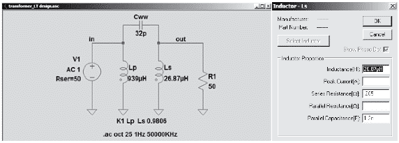
- In this case: Parallel capacitance corresponds to Cwsec
- Series resistance corresponds to RCusec
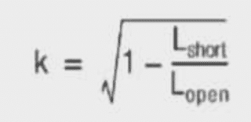
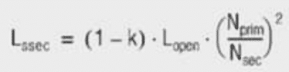
- The coupling factor is calculated from:
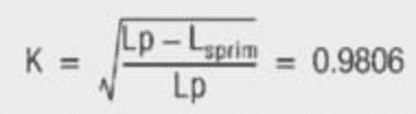
(with Ls: 939 µH; Lssec:36.5 µH) and then enter in the LTspice text editor as SPICE DIRECTIVE.

Further calculation formulas for the equivalent parameters for the model with main inductance Lm:

From this follows for the different inductance:


The values for the resistances are determined by simple measurement with the ohmmeter. This model does not consider core losses, any capacitance or the frequency dependence of resistances due to the skin and proximity effects.
Transformer Application Requirements
As illustrated with the transformer equivalent circuit, transformers have numerous parasitic properties, which can have a negative effect on the signal. In this chapter it is therefore explained why and where one applies transformers. An additional section deals with the requirements for signal transformers. To conclude the chapter, some standard commercially available transformers are described.
Function and Application Areas of Transformers
As a result of their functionality, transformers can be used for various tasks:
- Isolation: Transformers are constructed of several windings. Depend ing on the additional isolation, various potentials can be separated or isolated from one another
- Voltage transformation: Voltages are transformed proportionally to the turns ratio
- Current transformation: Currents are transformed inversely to the turns ratio (see chapter I/1.9)
- Impedance matching: Impedances are transformed as the square of the turns ratio
This gives rise to various applications for transformers:
- Voltage (power) supplies: Here the main functions of the trans former are voltage transformation and isolation
- Current converters: Here the main function is to convert high currents into small measurable currents
- Pulse transformers, e.g. drive transformers for transistors: The main function is isolation; sometimes higher voltages are also required to drive a transistor
- Data transformers: Here the main function is also isolation. In addition, sometimes different impedances have to be matched or voltages increased.
Requirements for Data and Signal Transformers
Transformers are used on data lines mainly for isolation and impedance matching. The signal should be largely unaffected in this case. The magnetizing current is not transferred to the secondary side. For this reason, the transformer should have the highest possible main inductance.
The signal profiles are usually rectangular pulses, i.e. they include a large number of harmonics. For the transformer, this means that its transformation properties should be as constant as possible up to high frequencies. Taking a look at the transformer equivalent circuit at the previous chapter, it is apparent that the leakage inductances contribute to addition frequency-dependent signal attenuation. The leakage inductances should therefore be kept as low as possible. Signal transformers therefore usually deploy ring cores with high permeability. The windings are at least bifilar; wound with twisted wires is better still. Because the power transfer is rather small, DCR is of minor importance.
The direct parameters, such as leakage inductance, interwinding capacitance etc. are usually not specified in the datasheets for signal transformers, but rather the associated parameters, such as insertion loss, return loss, etc.
The most important parameters are defined as follows:
• Insertion loss IL: Measure of the losses caused by the transformer
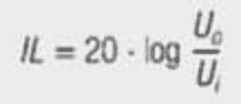
Uo = output voltage; Ui = input voltage
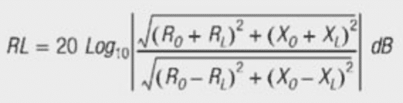
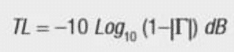
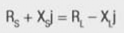
• Return loss RL: Measure of the energy reflected back from the transformer due to imperfect impedance matching
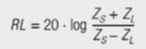
ZS = source impedance; ZL = load impedance
• Common Mode Rejection: Measure of the suppression of DC interference
• Total harmonic distortion: The relationship between the total energy of the harmonics and the energy of the fundamental
• Bandwidth: Frequency range in which the insertion loss is lower than 3 dB
A Transformer’s Effect on Return Loss
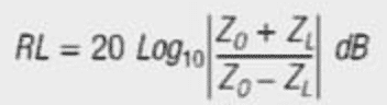
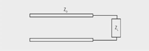
Return loss is an expression in decibels (dB) of the power reflected on a transmission line from a mismatched load in relationship to the power of the transmitted incident signal. The reflected signal disrupts the desired signal and if severe enough will cause data transmission errors in data lines or degradation in sound quality on voice circuits.
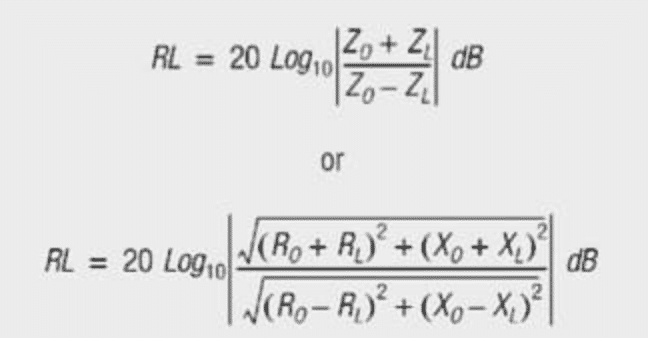
The equation for calculating return loss in terms of characteristic complex line impedance, ZO, and the actual complex load, ZL, is shown below in eq. [3]. Expanding the return loss equation to terms of resistance and reactance we achieve formula as per eq. [4]:
Since return loss is a function of line and load impedance, the characteristic impedance of a transformer, inductor or choke will affect the return loss. A simple impedance sweep of a magnetic component reveals that the impedance varies over frequency, hence the return loss varies over frequency. We will discuss further the effects of a transformer on return loss later. Now let’s explore the relationship of return loss to other common reflection terms.
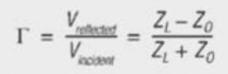
Reflection Coefficient
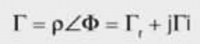
While return loss is generally used to denote line reflections in the magnetics industry; a more common term in the electronics industry for reflections is the complex reflection coefficient, gamma, which is symbolized either by the Roman character G or more commonly the equivalent Greek character Γ (gamma). The complex reflection coefficient Γ has a magnitude portion called ρ (rho) and a phase angle portion Φ (Phi). Those of you familiar with the Smith Chart know that the radius of the circle encompassing the Smith Chart is rho equal to one.
The reflection coefficient, gamma, is defined as the ratio of the reflected voltage signal in relationship to the incident voltage signal – see eq. 5 below.
Keep in mind that just as impedance is a complex number, so is gamma and it may be expressed either in polar format with rho and Phi or in rectangular format:
Return loss expressed in terms of gamma is shown in the equation [7] below:

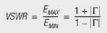
Standing Wave Ratio
The reflections on a transmission line caused by impedance mismatches reveal themselves in an envelope of the combined incident and reflected wave forms. The standing wave ratio, SWR, is the ratio of the maximum value of the resulting RF envelope EMAX to the minimum value EMIN.

The standing wave ratio expressed in terms of the reflection coefficient is shown below:
Transmission Loss
The last signal reflection expression that we will discuss is the transmission loss. Transmission loss is simply the ratio of power transmitted to the load relative to the incident signal power. Transmission loss in a lossless network expressed in terms of the reflection coefficient is shown below:
Don’t forget that the magnitude of gamma (|Γ|) is rho (ρ) and either form can be found in publications and documents regarding reflections.
Related Terms
Reviewing the complex reflection coefficient formula we can see that the closer matched the load impedance ZL is to the characteristic line impedance ZO the closer to zero the reflection coefficient is. As the mismatch between the two impedances increase the reflection coefficient increases to a maximum magnitude of one.
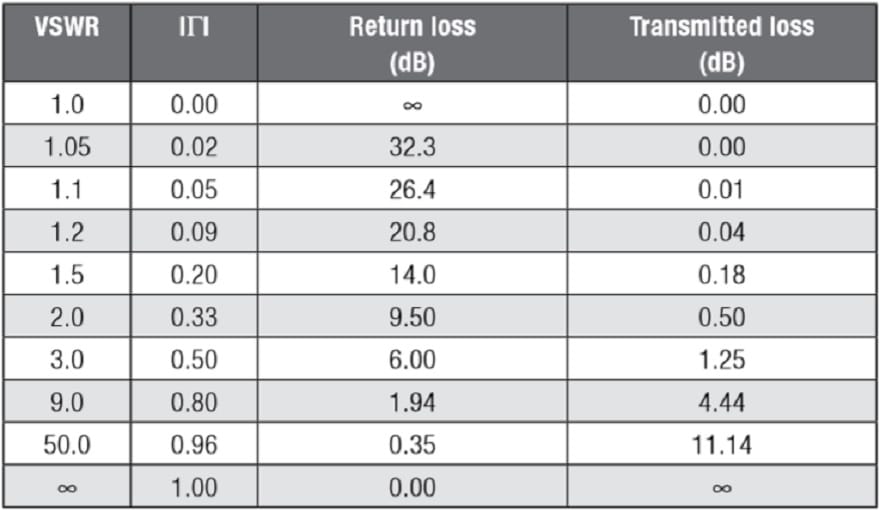
The table below shows how the varying complex reflection coefficient relates to SWR, return loss and transmitted loss. As can be seen a perfect match results in SWR equal to 1 and an infinite return loss. Similarly an open or short at the load will result in return an infinite SWR and 0 dB of return loss.
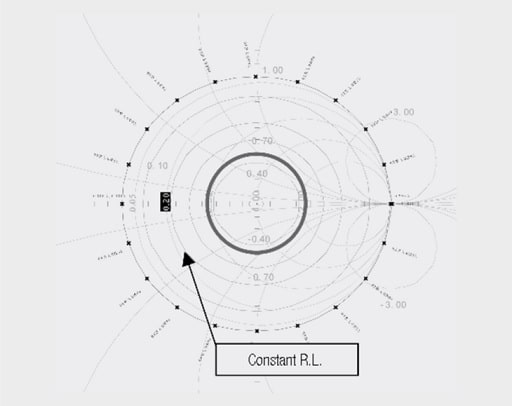
Plotted on a Smith Chart the relationship is even more evident as constant values of all four parameters are graphed on the chart as circles:
Maximum Power Transfer
Maximum power transfer is obtained from the source to the load when the source impedance is equal to the complex conjugate of the load impedance. This not only maximizes power but minimizes reflection energy back to the source.
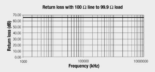
Return Loss with Matched Load
Let’s take an example of a matched line and load. Let’s say that ZO = 100 Ω in an ADSL application and that it is terminated with a purely resistive load of 100 Ω.
where: ZO = 100 + 0j Ω; ZL = 100 + 0j Ω
Since the load and source are purely resistive, the return loss will be the same at any frequency. Substituting and calculating shows that RL = ∞.
Return Loss with Unmatched load
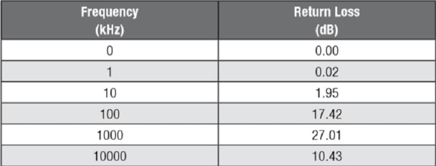
Let’s take the same example of an ideal transformer, but with a slightly unmatched load. Let’s say that ZO = 100+0j Ω as before, but now we will calculate return loss at a number of purely resistive load impedances to show how return loss if affected by mismatch. The resistive load is used again so that the return loss will be independent of frequency.

The results show that return loss is a function of mismatch and without regard to which direction the mismatch is in. If we look at the case of a slightly mismatched line versus load we see that it is independent of frequency if the line and load are purely resistive. Also note that if the match was perfect, the return loss would be infinite.
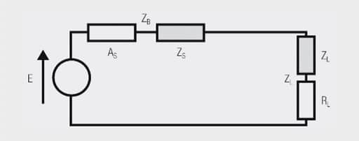
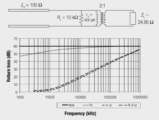
Return Loss with Nearly Ideal Transformer
Now let’s take the same example of a matched line and load, but add in a 1 : 1 transformer which is ideal except for having a primary inductance of LP = 600 µH. Again we assume the line impedance is a purely resistive 100 Ω as well as the load impedance.
When we had an ideal transformer with both line and load impedances purely resistive, our return loss did not vary over frequency and was the same at any frequency. Now however, the inductance will vary over frequency thereby causing the effective load to vary over frequency. The return loss calculation also becomes more complex due to the load impedance now being complex.
Rather than go through all of the complex impedance calculations, I will show the steps required to calculate the return loss.
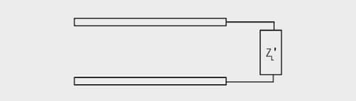
Step 1 : Using impedance transformation calculations, transform the impedance to the same side of the ideal transformer as the primary inductance. In this case the ideal transformer is a 1 : 1 transformer and the load does not change. See Figure 16.
Step 2: Combine the XL the current ZL = RL+0j with a resultant ZL’ which is complex.
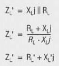
Step 3: Calculate return loss using the resultant load and the original resistive line impedance as per eq. [4].
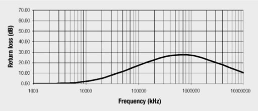
Results: Looking at the results over frequency we can see that the inductance at the lower end is mismatched due the inductance shorting out the load. The lower the primary inductance the more the load will be shunted. Looking at the graphed results we see that return loss due to the primary inductance will behave much like a filter in that it has a knee which will vary with inductance and the slope after the knee is 20 dB per decade.

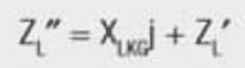
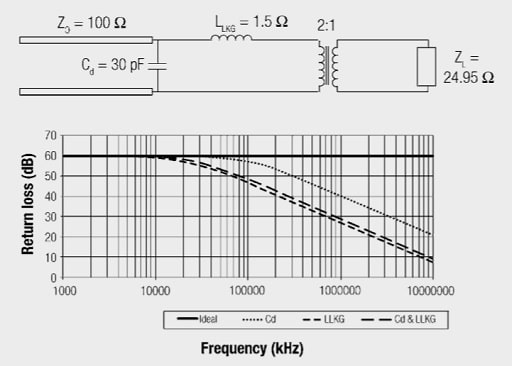
Return Loss with Leakage Inductance Added
Consider return loss with leakage inductance as shown in Figure 19. Now let’s add leakage inductance of 1 µH to the same transformer under the same load conditions (Figure 20.). The effective load is calculated in the same manner with ZL’ the reactance of the primary in parallel with the load impedance after transformation. The ZL’’ is ZL’ with the series leakage inductance reactance added to it.
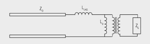

Using the same return loss formula we can then calculate our return loss at various frequencies. From the graphed results we see that the high frequency return loss is affected by the leakage inductance.
For most transformers the primary and leakage inductances will have the greatest effect on return loss, providing that the turns ratio chosen effectively matches the load resistance to the line impedance.
Return Loss with a Less-Than-Ideal Transformer
With the linear transformer model that is typically used in low frequency transformer design applications, we can calculate theoretical return loss based on lumped parameter analysis. With the exception of inter-winding capacitance, we can reduce the linear transformer model to a load impedance by either combining the elements in parallel or series. Keep in mind that the secondary DC resistance and the ZL have to be transformed by dividing by n2 when brought to the line side of the model.
Inter-winding capacitance can not be so simply modeled because it resides on neither the line nor the load side of the model and can not be transformed into the equivalent load. At low frequencies the inter-winding capacitance acts as an open across the transformer and typically can be ignored. In fact most modeling programs for transformers do ignore inter-winding capacitance as leakage inductance and primary inductance are the dominant elements. However in certain designs where inter-winding capacitance is fairly large and the operating frequencies are high, it can become a very significant factor. Suffice it to say that if inter-winding capacitance needs to be included in the model it would be wise to use a more sophisticated analysis program such as LTspice.
Let’s take a look now at the linear transformer model for the theoretical ADSL transformer shown below with a load that is just off of the ideal 25 Ω for a perfect match. We will take this and model the effect of the various elements looking at it parameter by parameter.

Return Loss Effect of DCRs
The return loss effect of the DC resistance in the example on Figure 24. high lights two observations. First of all even though the secondary resistance is lower at 1.5 Ω in comparison to the primary resistance of 3.0 Ω, the effect on return loss is much greater. The reason for this is that the 1.5 Ω secondary when reflected to the primary side of the transformer is seen as 6.0 Ω.
Also note that a lower return loss number is only slightly affected by other elements that have significantly better return loss when standing alone. The return loss when due only to the secondary resistance is roughly 30 dB while the return loss due to the primary resistance is roughly 37 dB. When combined, the net effect is a return loss of 27 dB.
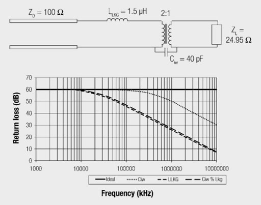
Return Loss Effect of Leakage Inductance and Distributed Capacitance
The effects on return loss by the leakage inductance and the distributive capacitance parameters of a transformer are interesting to compare as well. We see from the example on Figure 25. that the effects due solely to leakage inductance reveal a decaying return loss at the rate of 20 dB per decade. Now taking a look at the distributed capacitance we see that it causes a high-end decay at the same rate with the knee at a higher frequency.
The comparison gets interesting when we looked at the combined affect. When combined the net result is an improvement of return loss. Why is this? If you remember in our previous discussion, the return loss is a function of mismatch without regard to which direction the mismatch is in. With this example the mismatch is in opposite directions so the addition of the distributed capacitance effect actually improves the overall return loss.
Thinking about this in analytical terms, what is happening in the equivalent circuit? The reflected load is being increased by the reactance due to the leakage inductance thereby causing mismatch. However the reactance of the distributed capacitance is in parallel there by reducing the mismatch back toward the optimal 100 Ω reflected load.
Return Loss Effect of Inter-Winding Capacitance
As mentioned earlier, the effect of inter-winding capacitance is very difficult to calculate using simple equivalent impedance transformations. The problem is that the inter-winding capacitance is shared by both windings and is not clearly on one side of the ideal transformer or the other. The impact to the circuit model is therefore not so straight forward and requires more sophisticated modeling techniques. The example below was modeled with PSPICE rather than with simple calculations.
Typically however, the inter-winding capacitance has very little effect on the return loss in comparison to the leakage inductance and can be ignored. A word of warning is in order however since cases where leakage inductance is very low while at the same time the inter-winding capacitance is very high, inter-winding apacitance can become a factor to reckon with. See figure 26.
Return Loss Effect of Resistive Core Loss and Inductance
In this example we compare return loss due to the primary inductance as well as to the resistive core loss assuming that core loss factor, RcAlpha, is equal to 0.44. As can be seen from the return loss due to the combined effect, the resistive core loss has very minimal impact. In very low frequency applications, such as audio, the resistive core loss can be a factor.

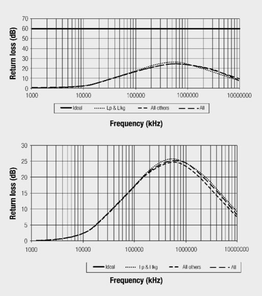
Return Loss Effect of All Parameters
Finally, looking at the effects of all parameters combined (Figure 28.) we can determine which are the significant factors in a typical transformer application. As can be seen from the results below, the leakage inductance and the primary inductance are the driving factors. While the other parasitic parameters do play a role in shaping the return loss response, they play a relatively minor role in a typical transformer design.
A Closer Look at Dominating Parameters
In closing we take a closer look at the dominating parameters of the transformer. The top graph on Figure 29. shows the return loss of various models in comparison to the ideal transformer with the slightly mismatched load. Then the lower graph on Figure 29. just zooms in on the non-ideal transformer cases.
Practical tip:
These graphs high-light the fact that primary and leakage inductance are the parameters that typically dictate return loss and that there is justification to ignoring inter-winding capacitance in most applications.
LAN, Telecom and Power Transformers
LAN and LAN RJ45 series Ethernet transformers
The LAN Ethernet transformers (Figure 30.) are not simple transformers, but rather modules in which, depending on the number of ports for which they are suitable, at least two transformers and a certain number of current-compensated chokes are contained.
As the name denotes, they are designed as transformers for Ethernet networks. Ethernet is the most widespread form of local network (Local Area Network – LAN). Ethernet is operated at different transmission speeds. The requirements for Ethernet are described in the IEEE802.3 standards:
- 10 Base-T: transmission rate 10 Mbps > standard IEEE802.3
- 100 Base-T: transmission rate 100 Mbps > standard IEEE802.3u
- 1000 Base-T: transmission rate 1000 Mbps > standard IEEE802.3ab
- Power over Ethernet: independent of the transmission rate > IEEE802.3af
For these standards, the transmission medium is a copper cable with unshielded, twisted pairs (UTP) of type CAT5 or better. The other IEEE802.3 series standards refer to glass fibre cable transmission.
For 10 Base-T and 100 Base-T, one wire pair is used for the transmission channel (transmit) and one for the reception channel (receive). Two of the four wire pairs in the Cat5 cable remain unused. In the case of 1000 Base-T, all four wire pairs are used in both directions.
According to the EN60950 standard (safety of information technology equipment), Ethernet is classified as a TNV 1 circuit (telecommunication network voltage). It has to be isolated against a SELV circuit (safe extra low voltage). The test voltage stipulated by the standard must be at least 1.5 kV with a test duration of 1 min.
As a result of this isolation voltage, it is essential to use a transformer between the network and the Ethernet terminal device. So two transformers are required for 10/100 Base-T networks and four transformers for 1000 Base-T networks. The necessary number of transformers is integrated in the WE-LAN series modules. As described in the previous section, ring core transformers are used.
To avoid further external components, e.g. current-compensated chokes (data line filters), these are also integrated in the transformer modules (see Figure 31.).
The relevant Ethernet standards for 100 Base-T call for transformers with a minimum inductance of 350 µH and DC current premagnetisation of 8 mA. This should serve to ensure functionality even with small asymmetries of the wire pairs.
The turns ratio is defined by the Ethernet controller used. Whereas 10 Base-T often uses turns ratios of 1 : 1.414 or 1 : 2.5 on at least one of the lines, 100 and 1000 Base-T almost exclusively work with a turns ratio of 1 : 1. This is because the number of secondary turns is so large – due to the high primary inductance combined with a higher number of turns than with 10 Base-T – that they can no longer be accommodated on a small ring core. Winding with twisted wires is also no longer possible, which can still be tolerated for 10 Base-T, but leads to a deterioration in transmission properties for 100 Base-T.
The minimum insertion loss and the maximum values for return loss, cross-talk and common mode rejection are also defined over the entire frequency range.
Telecom Transformers
xDSL Digital Subscriber Line transformers
The xDSL Digital Subscriber Line transformers (Figure 33.) are specialized line interface transformers that are designed to optimise the performance of DSL chipsets. With each chipset varying in power drive levels, impedance characteristics and signal spectrum the transformers are very much chipset dependant in their design.
DSL (Digital Subscriber Line)
DSL technology has its origins in the competition between the telecom and cable television industry to offer each other’s services; video and data services. While the hybrid fiber/coax cable network was already a high-bandwidth network, the telecom industry had to look to some other technology to increase the bandwidth of their aging analog network.
ADSL (Asymmetrical Digital Subscriber Line)
The ADSL technology formed the backbone of the telecom industry’s initial foray into the high speed data and video services market. Asymmetrical in nature, the ADSL technology reserves the bulk of the available bandwidth for down loading data rather than uploading. This is consistent with the requirements of video services as well as the traffic pattern of the typical internet user. ADSL data rates generally are in the 1 to 16 Mbits/s downstream and 1 to 2 Mbit/s upstream with POTS service concurrently available on the same line. Various flavours and generations of ADSL are, and have been, promoted such as ADSL2, ADSL2+, ADSL+, RADSL, etc.
HDSL (High-Speed Digital Subscriber Line)
Following on the heels of ADSL technology was HDSL which addresses the needs of those users requir ing a symmetrical service with as much bandwidth available for upstream data traffic as downstream. The HDSL services are targeted to service providers, businesses and Small Office Home Office (SOHO) customers. Generally speaking the HDSL technology is a replacement for the older T1/E1 technology. Like ADSL, the HDSL technology is promoted in a host of variants such as SHDSL, SDSL, HDSL-2, HDSL-4 MDSL, IDSL, g.SHDSL etc.
VDSL (Very High Speed Digital Subscriber Line)
The latest generation DSL technologies are the VDSL and VDSL2 technologies. VDSL and VDSL2 increases the maximum available download bit rate to over 100 Mbit/s at short loop lengths. VDSL technologies allow for either symmetric or asymmetric access and support high bandwidth applications such as HDTV in addition to telephone and data services.
Transformer Key Parameters
Inductance:
Inductance requirements vary widely between not only DSL technologies, but also between chipsets. ADSL and VDSL inductance requirements can be below 100 µH while HDSL inductance specifications are over 3 mH. Depending on the specific requirements of the chipset this inductance can be any value in between and is almost always toleranc ed to a level of ± 5 to 10 percent. The inductance specification is almost always specified by the IC manufacturer and is dependant on a host of conflicting requirements including:
- The transformer’s need to handle DC current
- Whether or not the transformer has to perform a filtering function for concurrent POTS operations
- Signal bandwidth
- The insertion loss
- The return loss characteristics
- The impedance characteristics of the chipset
Leakage inductance:
Leakage inductance requirements are almost always held to a maximum value. In rare instances where the chipset is particularly sensitive to variations in impedance, the leakage inductance will be held to a tolerance requirement. While this is possible to achieve, it does result in a design that is very susceptible to variations in manufacturing and should be avoided if at all possible. Factors that dictate the leakage inductance specification include:
- The insertion loss requirements
- Signal bandwidth
- The return loss characteristics required
- The impedance characteristics of the chipset
DC resistance:
Besides affecting the power transfer efficiency of the transformer, DC resistance also affect to a lesser degree these DSL line transformer requirements:
- The insertion loss requirements
- The return loss characteristics
- The impedance characteristics of the chipset
- Longitudinal balance
Crosstalk:
While crosstalk is always a concern for IC manufacturers, it is typically not an issue with the line interface transformers. Almost all line interface transformers for DSL are constructed on some EP style of core which is by virtue of its’ shape, self shielding.
Voltage/safety isolation:
Voltage/safety isolation is always a consideration as it is the primary purpose of the DSL line interface transformer in the first place. Depending on the safety agency requirements and intended application the isolation as well as creepage and clearance requirements for the transformer will vary. Typically transformers need to supply basic or supplementary isolation for a working voltage of 250 V per the IEC60950 standard. In summary each of these parameter affect the others to a greater or lesser degree. The crux of DSL line interface design is balancing all of these parameters to create a solution that meets the customer requirements in a cost effective manner.
DC current handling:
Typically only HDSL type technologies require the transformer to operate with a DC current applied through the transformer. This requirement is due to the fact that HDSL type equipment is often called on to provide power to remote terminal devices. Typical DC current requirements for HDSL products are 60 to 100 mA.
Turns ratio:
Turns ratios, like inductance, can vary greatly from chipset to chipset. While most transformers have a single primary and secondary winding, it is not uncommon for some chipsets to require separate secondary windings for transmit and receive or even a separate auxiliary winding. Factors affecting the turns ratio include:
- The architecture of the chipset
- The return loss characteristics required
- The impedance characteristics of the chipset
- Whether or not the signal voltage needs to be stepped up or down
Inter-winding capacitance:
Inter-winding capacitance may or may not be specified by the IC manufacturers when defining the transformer requirements depending on the transceivers sensitivity to capacitance. However, regardless of whether or not it is specified, inter-winding capacitance affects the overall performance and is typically limited by the following requirements:
- The insertion loss
- Signal bandwidth
- The return loss characteristics
- The impedance characteristics of the chipset
- Longitudinal balance
Total harmonic distortion:
General: The total harmonic distortion THD denotes the ratio of the effective value of all harmonics of a signal to the effective value of the total signal.
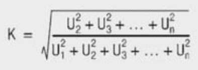
For sinusoidal signals, the total harmonic distortion is used as a measure of non-linear distortions! The smaller the THD, the more the signal corresponds to the original!
Total harmonic distortion is a measure of how much the DSL transformer will distort the desired signal. The harder a transformer is driven, the more the core approaches saturation. As the core approaches saturation the signal begins to distort. While total harmonic distortion is a concern for all DSL transformer, it is not as critical for VDSL transformers where the operation of the core is at higher frequency; hence a lower flux density and further away from saturation. HDSL transformers however utilize the lower end of the frequency bandwidth quite extensively and are often driven quite hard at these frequencies for longer loop lengths. This results in a need for good total harmonic distortion characteristics at a high flux density level.
Power Transformers
Power FLEX transformers
The FLEX transformers (Figure 34.) are especially well suited for DC-DC converters in the lower power rang. As a result of their winding structure, consisting of six individual windings each with the same number of turns, as well as the various air gaps available, the Flex transformers are very flexible in their application. Table 5. shows example of different sizes
The appropriate connections wiring of the windings on the circuit board allows various inductance and transformers with different turns ratios to be generated (Figure 36.).
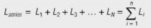
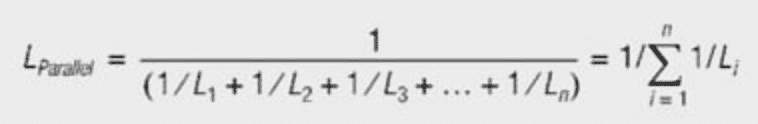
When calculating the resulting currents and inductance, it must be kept in mind that the six windings are wound on the same core – so they are magnetically coupled. Connecting two discrete inductance in series, the inductance are added (Equation [11]). Connected in parallel, the reciprocal values of the inductance add together (Equation [12]), i.e. connecting two equal inductance in parallel produces half the inductance.
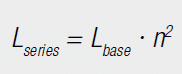
Connecting windings to a common core means adding the number of turns. These are squared in the calculation of the resulting inductance. As the number of turns of the single windings for WE-FLEX is identical, the resulting inductance is proportional to the square of the number of windings connected in series (Equation [13]). For parallel connection, the number of turns stays the same; only the conductor cross-section changes. So with parallel connection there is no change in inductance (Equation [14]).

Lbase Inductance of a Winding
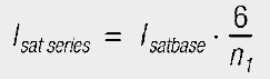
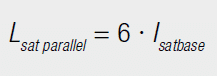
To determine Isatbase all six windings were connected in parallel and the inductance measured as a function of current. The saturation current determined in this way is the total saturation current of the component. Isatbase is then the measured saturation current divided by six.

Consequently, the total saturation current of the transformer is six times Isatbase. This total saturation current can now be distributed over the current-carrying windings. If, for example, three windings are connected in series, the six times Isatbase can be distributed over these three windings. Hence, each of these windings may carry current of twice Isatbase.
In the case of parallel connection of three windings, these can also carry twice Isatbase. For parallel connection, the individual currents add together to produce the total current, six times Isatbase. The following rules generally apply:
nI Number of Current-Carrying Windings
In contrast, the rated current, which is a property of the wire diameter, cannot be distributed to other windings. The resulting rated current for series and parallel connections is given by the following formulas:


The saturation current is not crucial when it comes to dimensioning transformers as forward converters or push-pull converters, but rather the voltage-µs product. The voltage-µs product or Volt-µs product is proportional to the number of turns, so that the Volt-µs product from has to be multiplied by the number of windings connected in series.
The windings of the FLEX transformers are tested against each other with 500 VDC. There is no additional insulation layer between the individual windings, so they can only be used in the low voltage range (SELV: < 60 VDC).
PoE Series Power-over-Ethernet Transformers
A DC-DC converter is also required for the power supply in Power over Ethernet. This has to satisfy the following tasks:
- PoE dialogue for detection and power classification
- Voltage regulation to the required output voltage
- Isolation of 1.5 kVAC in accordance with EN60950
Only a DC-DC converter with a transformer meets the isolation requirement. The leading semiconductor manufacturers have developed ICs that implement both the PoE dialogue, as well as voltage regulation. Examples of these include LTC4267 (Linear Technology), LM5071 (National Semiconductor) and TPS23750 (Texas Instruments). These ICs were developed for flyback converters with switching frequencies of between 200 und 400 kHz.
The transformers are tested with 1.5 kVAC between the primary and secondary sides and therefore comply with the international standards EN60950 and IEC60950.
UNIT offline transformers
The UNIT transformers (Figure 38.) are designed for worldwide mains input voltages. The input voltage can span the range from 85 VAC (e.g. Japan) to 265 VAC (e.g. Germany). In contrast to 50 Hz transformers, which have to be switched from 110 V to 230 V, the modern switch mode power supplies regulate this. At the same time optimized IC switching regulators are available and make the requests for low standby losses possible.
A switched DC voltage of 120 V to 385 V is applied at the transformer. Many IC manufacturers have brought ICs in the low power range onto the market in which MOSFETS are already integrated. Consequently the circuit complexity and the amount of external components is minimized.
CST Current Sense Transformers
There are two modes of regulating the output voltage of a switched mode power supply. For voltage regulation (Voltage Mode, VM), the output voltage is measured directly and compared with a “reference voltage”. For current regulation (Current Mode, CM), the primary current is measured. The output voltage serves as a reference here.
To measure the primary current, the voltage can be tapped by a sense resistor. A current converter is often used for a higher primary current so that losses are not too high. The current is then determined with a burden resistor RT by measuring voltage (Figure 40).
The voltage measured at RT is given by:
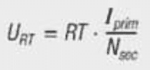
- URT = voltage at the burden resistor
- RT = burden resistor

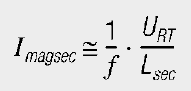
As described in the functionality of a transformer, a magnetizing current also appears here. This affects the result as a measurement error. The magnetizing current must therefore be considered when selecting a current converter. It can be estimated with the following formula:
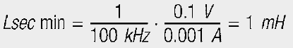
This is clarified with an example:
A current converter with the following properties is sought:
- Input currents: Ii = 1 A–5 A
- Frequency: f = 100 kHz
- Burden voltage: URT = 0.1 V at 1 A = 0.5 V at 5 A
- Accuracy: 10%
For a turns ratio of 1 : 100, Equation [16] gives a burden resistance of 10 Ω. The accuracy for the input current of 1A should be better than 0.1 A, i.e. the magnetizing current carried over to the secondary side must be smaller than 0.001 A. Equation [18] calculates the minimum inductance as: