Integrated Resistors
R 3.12 INTEGRATED RESISTORS
On ceramic boards integrated components are no novelty. Integrated resistors and capacitors are common in thick film and thin film circuits. The sheet resistivity of thick film resistors usually ranges from 10 Ω/square to 1 MΩ/square . Values down to 0.5 Ω/square and up to 1 GΩ/square are, however, quite possible. Generally one prints with a width of 0.5 to 1 mm (20 to 40 mils). Then sheet resistivity and element length (number of squares) determine the wanted resistance.
There are now thick film materials available that can be screen printed on polymeric substrates.
In recent years another method of integrating resistors is introduced that is called buried resistors technology. It is intended for large scale production and works with polymeric substrates on which are printed laminates that consist, at the bottom, of a resistive alloy and, on top, of an electrically conductive copper film.
The art work of the resistive elements and their terminals are produced by means of photoplot and etching. The resistive film consists of a nickel phosphorus alloy with sheet resistivities of 25 or 100 Ω/square and corresponding thicknesses of 0.4 and 0.1 mm (16 and 4 microinches). By arranging a number of such squares to a bar or serpentine geometry one can create resistance values of hundreds or thousands of ohms. A width may range between 0.2 and 2 mm (8 and 80 mils).
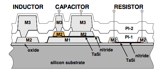
Integrated resistors and passives on silicon substrate
Integrated passive devices (IPDs) can be also created by semiconductor technology on silicon wafers.
Integrated passive devices are seeing greater use within system-in-package technology and numerous applications, including the Internet of Things. The tiny devices are making their way into automotive electronics, consumer electronics, and health-care products, among other uses.
Europe is leading the way in supplying IPDs, thanks to offerings from Infineon Technologies, STMicroelectronics, and Murata Integrated Passive Solutions (formerly IPDiA).
One of the big advantages here is that IPDs can reduce passive component sizes by up to 70%. Thin-film IPD technology using silicon or fan-out can provide a cost-effective solution, while providing improved performance for an SiP product. Silicon-based IPDs are a cost-effective technology produced in advanced 200-millimeter manufacturing facilities, and they’re ideal for system-in-package. IPD offers a competitive advantage in size, cost, and performance.”
IPD manufacturing comes in two flavors—thick-film IPD and thin-film IPD technologies. A thin-film-based integrated passive device is a silicon-based passive component integration. It’s a cost-effective way to reduce package footprint, reduce interconnection complexity, improve performance, component tolerance, improving your yields, and improving reliability. Applications are including RF modules, ultra-wideband, WLAN, handheld devices, cellular phones..
Some SiP have been able to replace 100 discrete components with two or three IPDs. More typically, a single IPD can take the place of 13 or 14 discrete devices.
STATS ChipPAC uses a wafer fabrication process for critical-dimension control. It offers a copper metallization process that deposits 8 microns or more of copper on a silicon wafer. Fabricating IPDs has typically involved a single dielectric layer of silicon nitride, but in next generation it may expanded in more layers.