
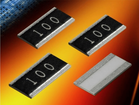
SMD Resistors
R 3.10.1 SMD Chip
The predominant part of all chips are manufactured with thick film, but thin film chips are becoming more and more common. Also metal foil exists as SMD. The construction is like the one in Figure R3-11. Certain types have an organic protection in one or two layers on top of the glass passivation.
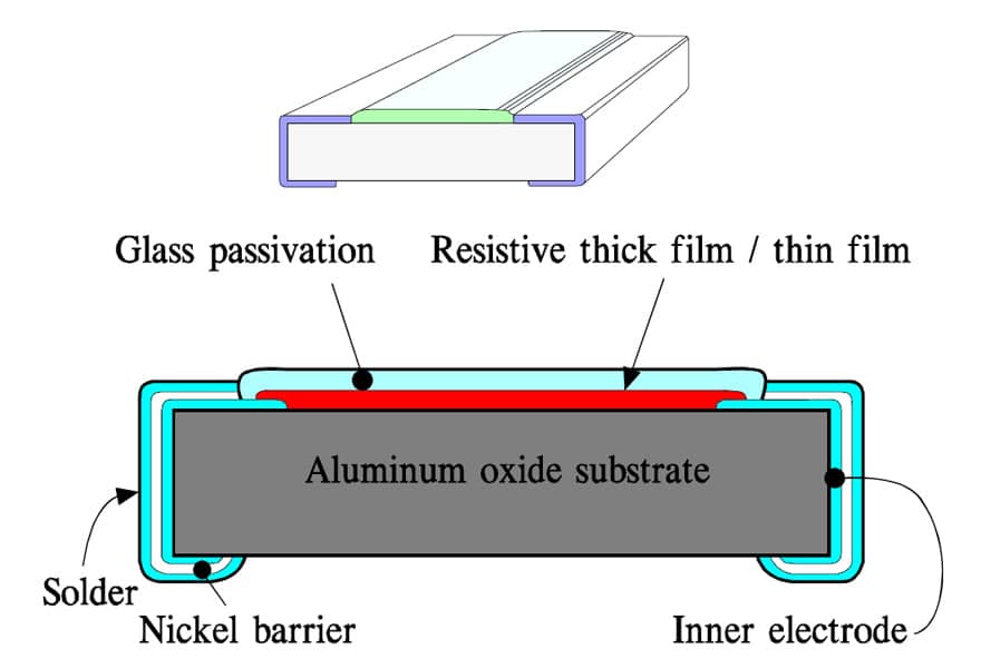
The substrates are screen printed either with a metal powder paste that is fired to a metal glaze / thick film. Or metal foils are glued on a substrate or metal films are vaporized or ion implanted on it.
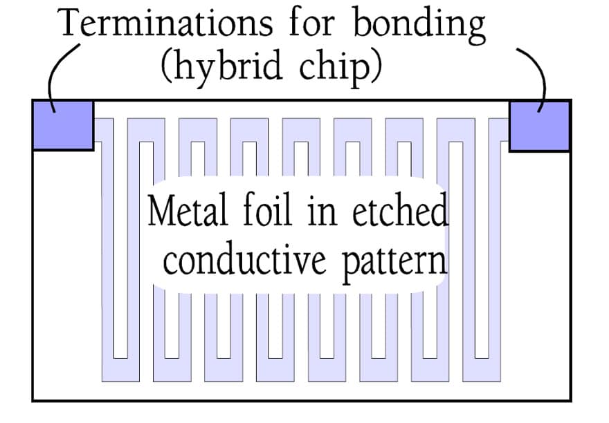
The thick film is laser trimmed to the right resistance value by cutting a track in the long side of the film. Recent manufacturing improvements however begin making this laser trimming unnecessary. This approach without any trimming tracks will increase the pulse load capability by 2 to 3 times. The other films are designed to an inductance-reducing serpentine pattern according to Figure R3-12.
The metal foil pattern is etched chemically or patterned by means of an ion beam. The thin metal films are applied through a mask to the desired shape.
Linear PTC designs in metal glaze are marketed. Typical data are, for example, 10 kΩ and TCR +1500 ppm/°C. Metal film chips with resistance track in a serpentine pattern also exist. Typical EIA sizes are 0603, 0805 and 1206. Common TCRs range from +150 to +4500 ppm/°C while the corresponding maximum resistance values drop from 50 kΩ to 500 Ω. The higher TCR the lower the maximum resistance which depends on the film alloys that more and more are approaching the pure metal and its correspondingly lower resistivity.
Metal foil chips exist in two designs, partly as the wrap-around according to Figure R3-11, partly for use in integrated electronics (Figure R3-12). In the latter case they are made with a protective glass passivation and with bonding pads which implies separate encapsulation.
A variant of bulk metal chips are used as current sensor. The resistance element consists of a metal plate that by laser cutting can be trimmed to tolerances of ±1% at resistance values in the range of 5 to 50 mΩ. The design and its tolerances require large chip dimensions (for example 0.4×0.2”).
Sometimes metal foil chips are delivered for special custom trimming by a scribed line.
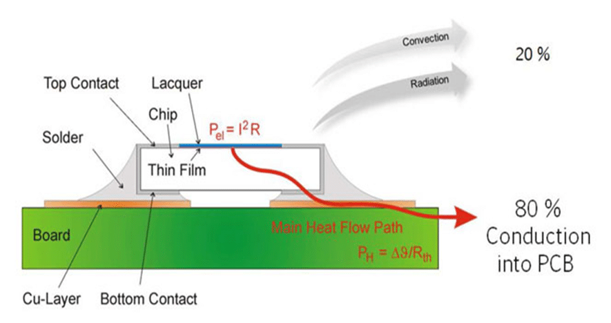
Power chip resistors exist in thick film design. Common power ratings are 1 or 2 watts. The resistance range may cover 10 mΩ … 22 MΩ with tolerances between 1 and 10 %. The heat generation requires dimensions in the magnitude of 12 x 8 or 8 x 5 mm. The terminations usually consist of tinned compliant copper plates.
Sizes
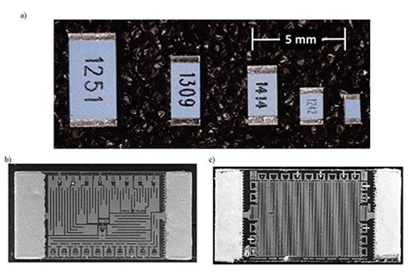
With thick film chips the main focus has been moved from the EIA size 0805 (2 x 1.25 mm) to sizes 0603 (1.6 x 0.8) and 0402 (0.8 x 0.5). Discrete thick film chips are marketed down to 0302 or 0201 (0.8 x 0.5 respectively 0.6 x 0.3 mm). The most common chip size in thin film technology is 20 x 20 mil (0.5 x 0.5 mm; EIA code 0202) but are also found conventional EIA sizes from 0201 to 2010.
Reverse Geometry
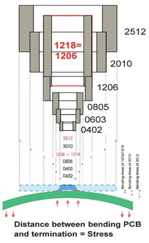
Similar to small chip capacitors, also SMD resistors are offered in “reverse geometry” variants with wider side of the chip as the terminals. The design benefits are in these fields:
- lower ESL = lower parasitic and higher frequency range
- better thermal conduction into PCB = higher power rating by 30-50%
- higher mechanical strength = higher vibration and flex stress robustness
- less thermal stress as differences in the coefficient of expansion between substrate and chip decreases in significance with shorter distances between terminations
The only downside of the design, considering the high manufacturing price is now almost identical, is a significantly more difficult PCB cleaning process in narrow and long gaps between the termination pads.