Resistor Networks
R 3.11 RESISTOR NETWORKS
R 3.11.1 General comments
Resistor networks are manufactured both for hole mount and as SMDs. Most parts are manufactured in thick film but thin film as well as metal foil types have a good market.
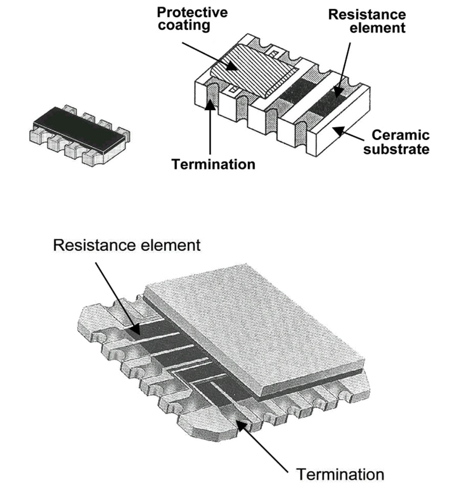
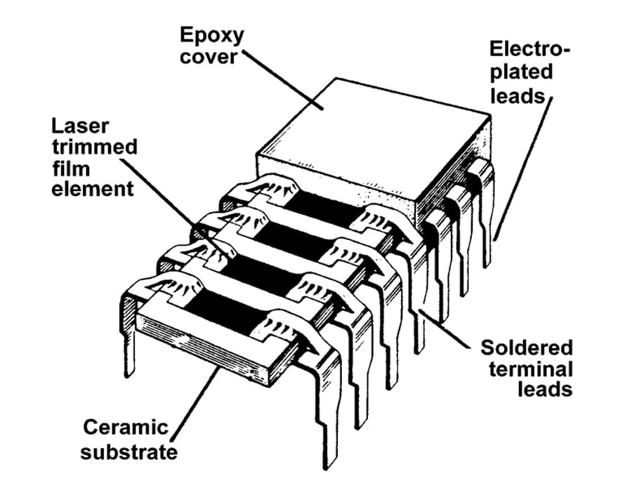
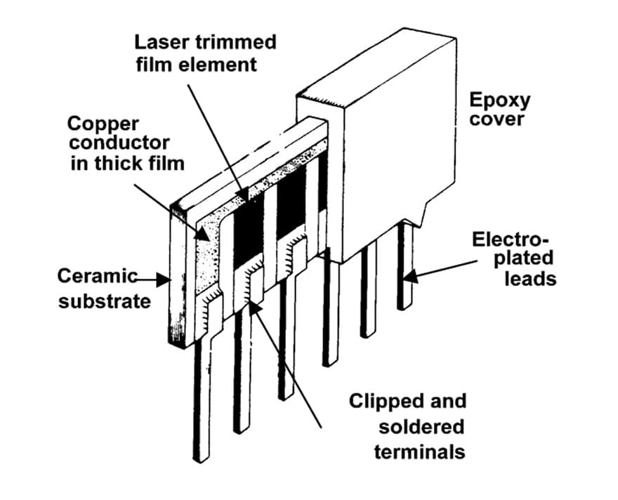
Discrete SM components may be mounted in the network package. But usually the planar substrates are screen printed with a network pattern either with a metal powder paste that is fired to metal glaze/thick film. Or metal foils are glued to the planar substrate or metal films of NiCr or Ta2N are vaporized or ion implanted – sputtered – on the substrates. The thick film is laser trimmed to the desired resistance value by cutting a track in one of the long sides of the film. However, just as with the discrete chips improved manufacturing technology begins making this laser trimming unnecessary. The other films are designed to a serpentine pattern which reduces the inductance of the element. The metal foils get their pattern by a chemical etching process or by means of the cleaner ion beam etching. The thin metal or metal oxide films are applied through a mask to desired shape.
Just as the chips the resistor element films are protected by a glass coat or sometimes a tantalum oxide coating.
R 3.11.2 Designs
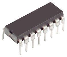
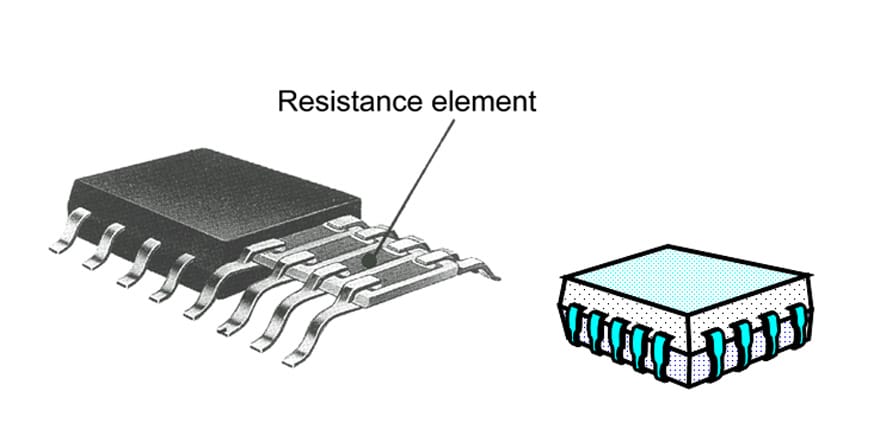
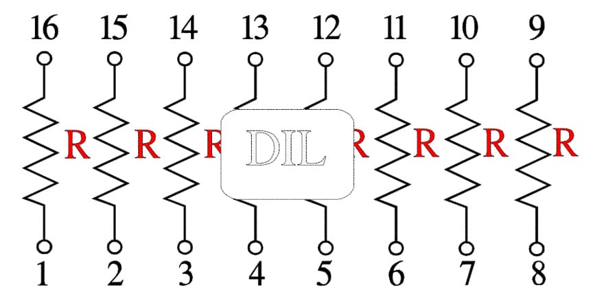
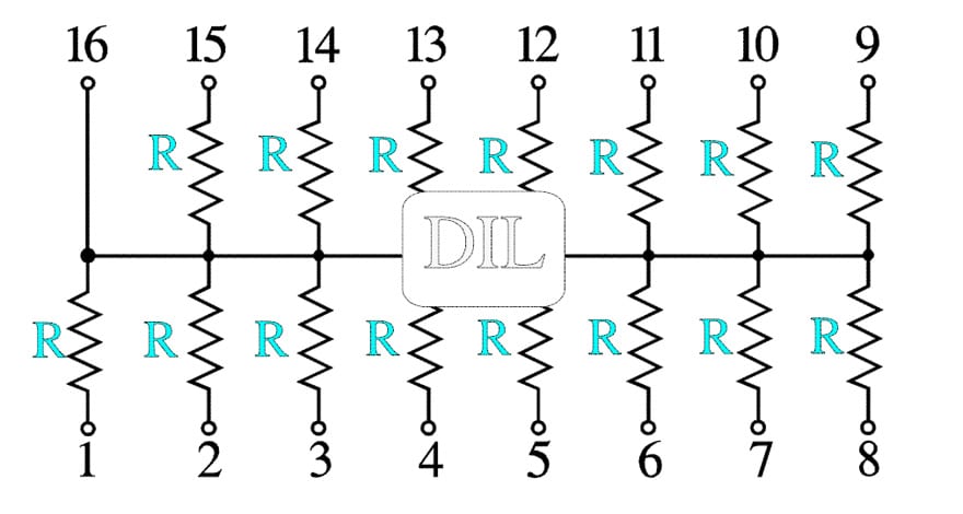
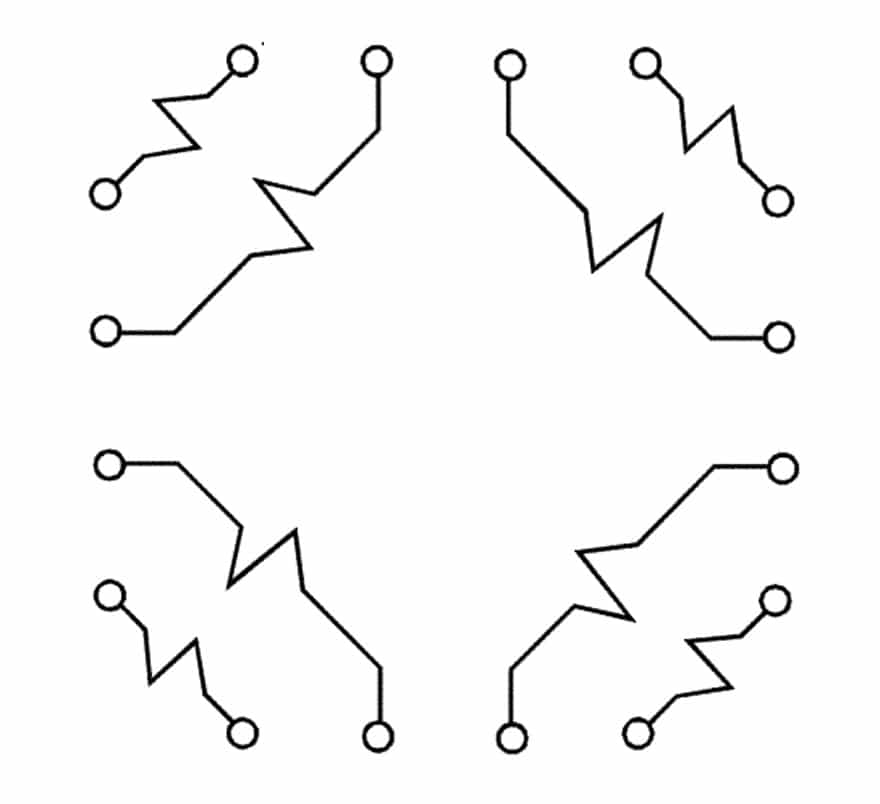
DIL (sometimes DIP) stands for Dual-In-Line respectively Dual-Inline Package (Figure R3-15). The number of leads varies; most common are 14, 16 or 18 leads.
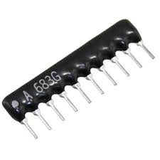
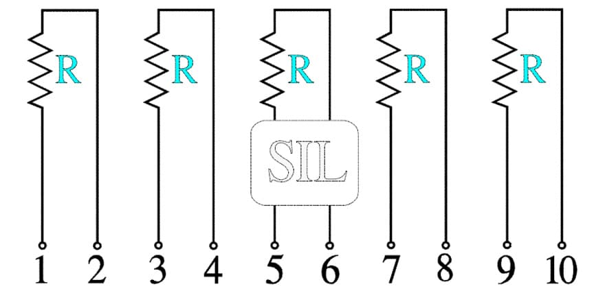
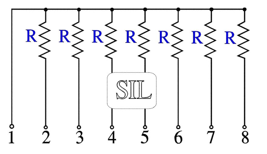
SIL or SIP means Single-In-Line respectively Single-Inline-Package. This network requires less surface but a higher building profile. It exists in the profiles 8 and 5 mm. The latter is most popular. A common number of leads are 4, 6, 8, 10 or 12 (Figure R3-16).
SMD networks exist in many different designs. Some are shown in Figures R3-13 and –14. . If the application implies considerable temperature changes examples like those in Figure R3-13 should, due to their lack of flexible leads, be mounted on ceramic substrates.
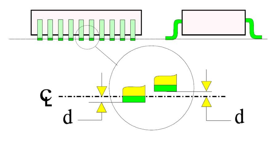
Of all requirements that have to be specified and checked there is one that is of particular interest: The coplanarity , i.e., the mutual planarity of the leads relatively to a reference plane. If this measure is not met – d in Figure R3-17 – some leads will be suspended in the air at soldering to the substrate. The measure is exemplified by the gull-wing shape but applies as well to the J hook design.
R 3.11.3 Configurations
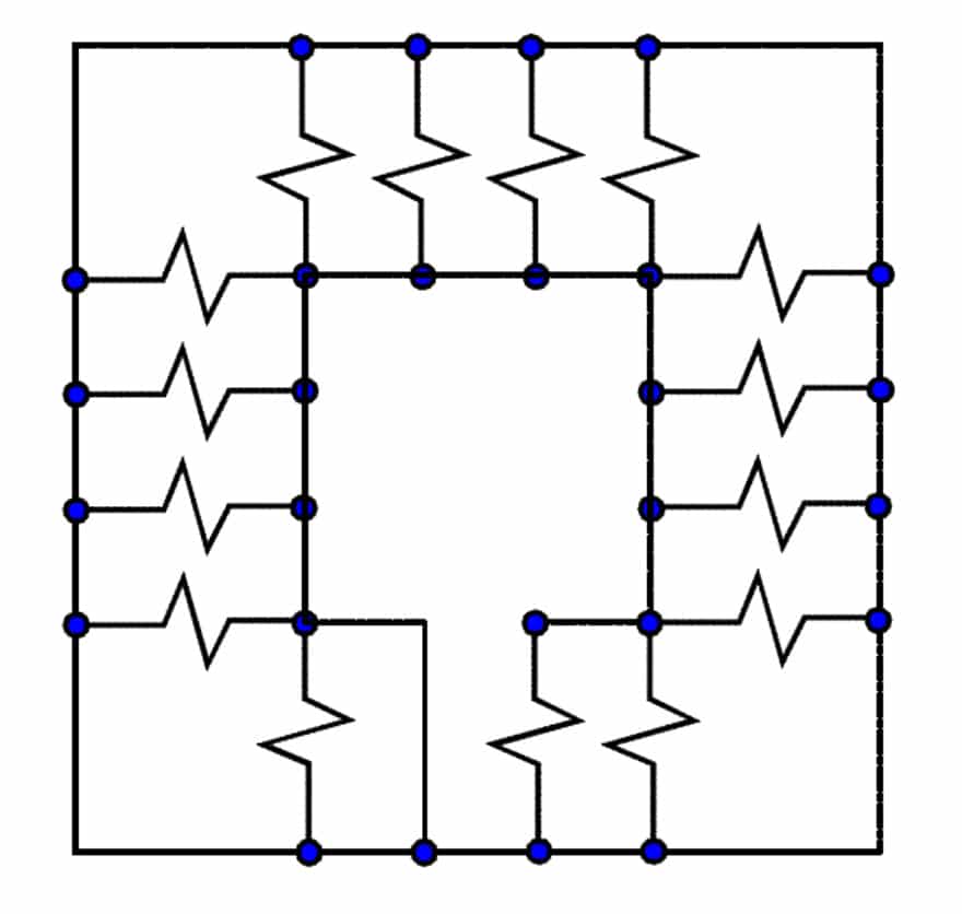
The electrical circuit can be arranged in an infinite number of ways. Usually the resistor values are mutually equal. Sometimes they are bussed (common neutral), sometimes they are arranged separately. Figures R3-18 to R3-23 show examples of the most common configurations.
R 3.11.4 Characteristics
In the first place the characteristics of the networks are determined by the resistor material that rules the TCR and the absolute tolerance. Because the elements included belong to the same manufacturing batch their parameter distribution is much more limited than that of the total production. This enables an additional kind of specification that often is used with precision components: the resistance ratio or relative tolerance and the TCR tracking. The concepts are illustrated in Figures R3-24 and –25.
In order to understand the resistance ratio concept better we should recollect how the absolute tolerance is constructed. If the actual resistance is called R and the nominal resistance Rnom, the ratio R/Rnom should be within the tolerance limits. With the relative tolerance, however, we mean a comparison of the different element resistances, Rr, with a reference element, Rref, in the network. Rref usually is the first element in the schematic.
The ratio Rr/Rref is called the resistance ratio accuracy, ratio tolerance (or relative tolerance) and is expressed in percent. It is a comparison of magnitude and therefore is given without a sign. If the element values of the network are distributed as in Figure R3-24 we realize that the largest spread will occur if Rref = Rmin and Rr = Rmax. Thus the resistance ratio accuracy, Rratio, shall fulfill the condition (Rmax – Rmin)/Rmin ≤ Rratio.
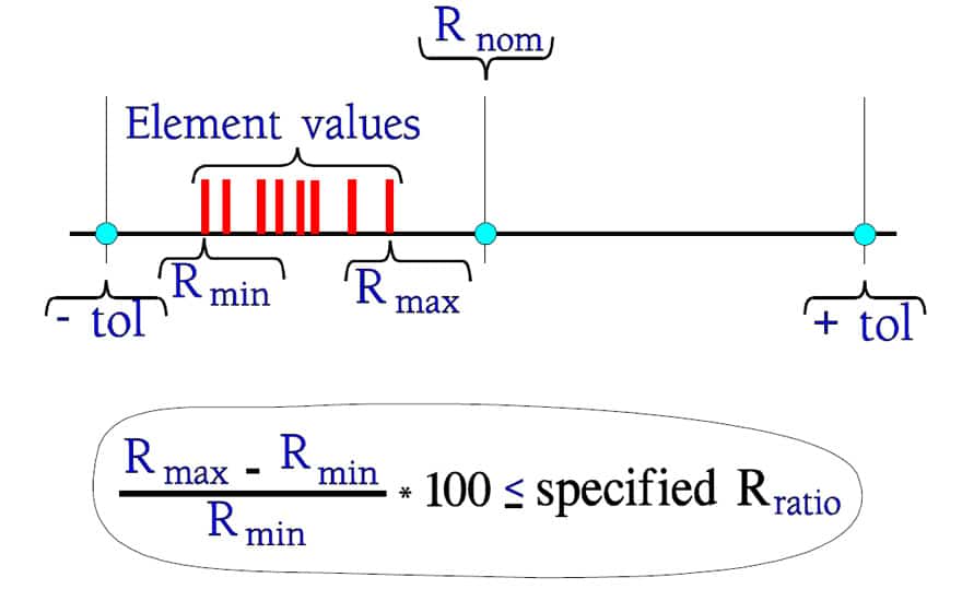
The resistance ratios may range over 0.2 to 2 % for the thick film networks and between 0.05 and 1 % for the thin film networks.
The TCR tracking, i.e., the reciprocal TCR differences between the elements, is illustrated in Figure R3-25.
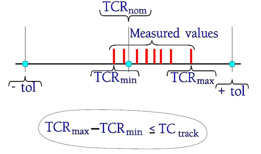
In practice the following rule of thumb often applies: TCRtrack ≈ ½ x TCRabs where TCRabs means specified absolute TCR.
TCRtrack for the thick film networks usually lies between 10 and 50 ppm/°C and for the thin film networks between 0.5 and 10 ppm/°C.
R 3.11.5 Failure modes
Soldering risks
Terminations with the usual pitch 0.1″ (2.54 mm) are subjected to a mutual thermal influence at soldering. For SMD networks there will in addition be the closeness to the substrate and the solder pads. Thus, networks run an increased risk of melting internal solder joints. Even if they will solidify after the soldering process there always is a risk of resulting dry joints. Usually this problem is avoided by specifying use of an internal solder with a melting point well above that of the external solder alloy.
Mechanical weaknesses
The ceramic substrates used often are relatively long and thin. Thermal and mechanical shocks as well as vibration may cause cracks in the ceramic under resistor elements and terminations and result in open modes that in the worst case are intermittent and temperature dependent (the nightmare of trouble shooting). Through hole mounted SIL networks run an extra risk of mechanical damage (if somebody, for example, wants to reposition a network that leans after soldering!).
Mechanically exposed designs sometimes are molded in epoxy, foamed plastic or equivalent. Even if the component surfaces are covered with a mould release agent that is in-
tended to prevent the molding compound to get hold of the components due to shape changes during the hardening process it doesn’t solve the problem with, for example, SIL networks. They are very easily exposed to unsymmetrical side forces that may crack the ceramic substrate.
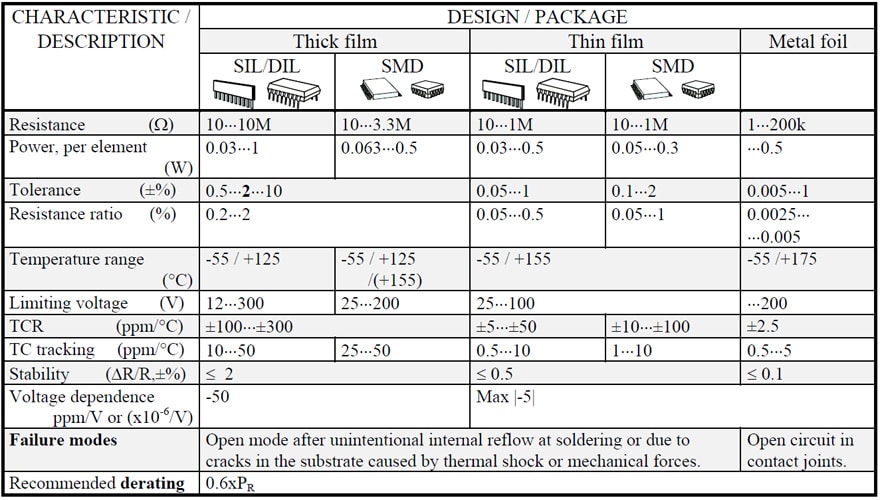
Table R3-8. RESISTOR NETWORKS