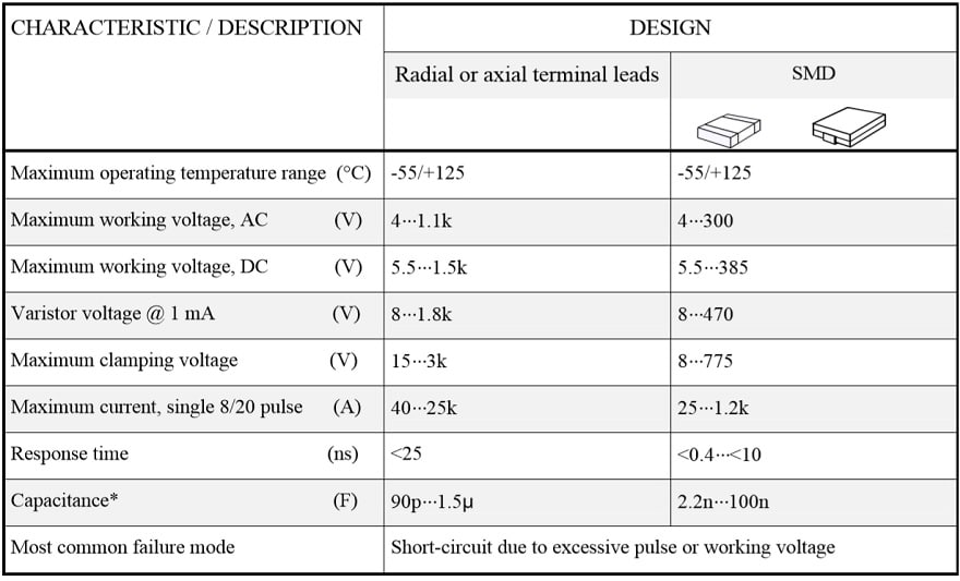
Varistors
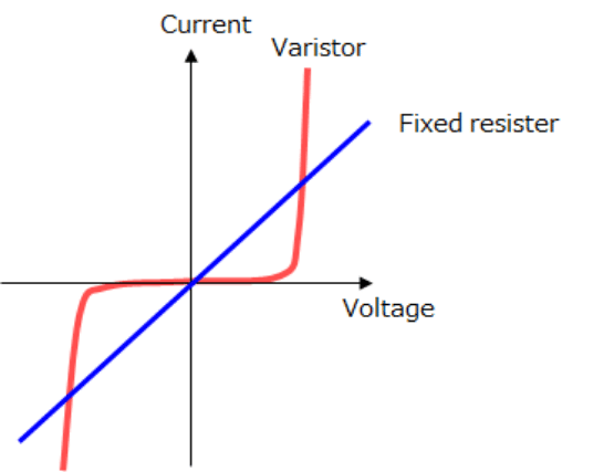
Varistor stands for Variable Resistor. It’s a voltage nonlinear resistor/voltage-dependent resistor. It is an element that changes its resistance value depending on applied voltage. This feature is mostly used to protect electronic devices from the abnormal voltage, such as lightning surge and static electricity. Unlike thermistors it has no practical time delay of its function.
R 5.3.1 Function and design
Just as thermistors the varistor is fabricated from a compressed and sintered powder compound that consists of silicon carbide (SiC) or zinc oxide (ZnO). The ZnO varistor has superior characteristics and predominates today all manufacture. This section deals with ZnO varistors only. If we sinter zinc oxide together with other metal oxide additives there is formed a polycrystalline ceramic. In the intergranular boundaries of the zinc oxide grains are formed P-N junctions with semiconductor characteristics – so called Double Schottky Barriers – with rectifying characteristics. Each ZnO grain with adherent boundaries acts as a miniature varistor with a symmetrical V/I characteristic. The grain compound can be regarded as a conglomerate of “microvaristors” connected in series and parallel. Thus the load and energy absorption capability in that way will be totally superior to conventional semiconducting elements. There the power generation exclusively will occur in the thin P-N boundary while in the varistor it takes place in all the microvaristors distributed homogeneously in the whole body.
The V/I characteristic of an elementary varistor may look like the one in Figure R5-24. Other manufacturers may have somewhat modified voltage values. The number of microvaristors connected in series and parallel determines the electrical characteristics of the varistor. If we connect 10 grains in series, with a characteristic according to the figure, we get a varistor with the thickness of 10 grains and a varistor voltage of 30 V. Varistors are shaped and encapsulated approximately as the thermistors.
Of the different designs discs are predominant, with radial leads and a variety of encapsulations, or with whole, metallized surfaces intended for series connection by piling the separate varistors. Encapsulations, for example lacquer or the like, require high tensional stability and resistance against washing agents. Of the uncovered types a certain tubular design intended for connectors should also be mentioned At manufacturing the goal is a grain compound with a regular structure, especially in high voltage/ high energy varistors.
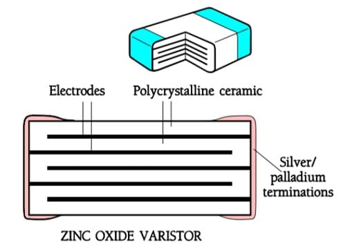
An irregular structure impedes the heat conduction and may lead to an uneven current distribution and occurring Hot Spots and local degradation of the material. In low voltage applications homogeneity is of vital importance. The combination of a multi-electrode construction and small, uniform grains has created the multilayer varistor (MLV), preferably used as SMD, intended for low voltage applications.
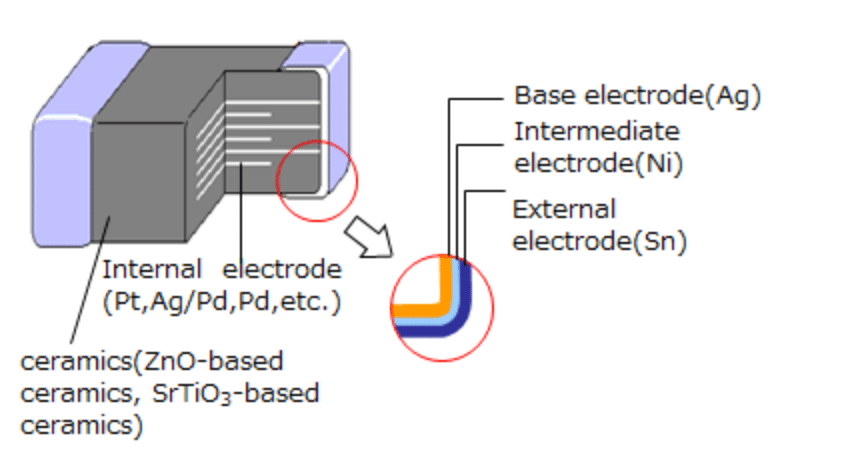
These MLVs are manufactured in a similar way as multilayer ceramics (MLCCs). The electrodes are screenprinted with a thick film ink on the zinc oxide layers, the layers are stacked to a pile with the desired number of layers. The stack then is sintered to a monolithic body and finally supplied with terminations that are fired onto the body ends. Silver or silver/palladium is used as termination metal in old and military styles (Figure R5-25) while BME nickel electrodes are the mass volume types today. Plating of a nickel barrier requires due to the conducting zinc oxide special processes which deviate from the conventional electroplating.
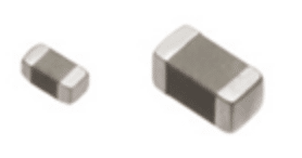
Multilayer SMD designs are produced in EIA sizes from 0201 to 2220.
R 5.3.2 Some definitions
Maximum working voltage
Maximum working voltage = the maximum voltage which continuously may be applied across the varistor.
Varistor voltage
The varistor voltage = the voltage across the varistor when a current of 1 mA is passed through the body.
Maximum clamping voltage
By maximum clamping voltage we mean the peak voltage across the varistor when it is subjected to a specified peak pulse current with a specified waveform. A common test pulse is the IEC specified so called 8/20 pulse with a specified current intensity.
Maximum transient peak current
The maximum current that may be allowed through a varistor depends on pulse shape and pulse width, repetition frequency and number of cycles. A starting point for the pulse capability is given by the maximum peak current of 8/20 shape that changes the varistor voltage with maximum 10 %. R
5.3.3 V / I characteristic
The V/I curve of the elementary varistor in Figure R724 differs slightly from that of the practical varistor that in the normal operation region might be approximated to
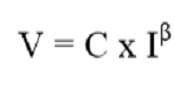
where:
C = varistor voltage at 1A.
I = actual working current.
β ≈ 0.03.
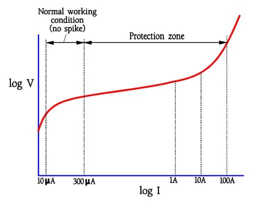
A typical V/I characteristic is shown in Figure R5-27.
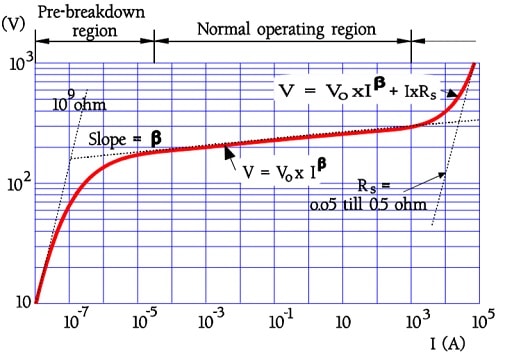
The V/I curve of a varistor has tolerances. When the leakage current is specified one presupposes the highest possible current at a certain voltage. The clamping voltage – the one occurring across the varistor when subjected to transients – is specified as the highest possible at a certain current. Thus the specifications are controlled by the unbroken line in Figure R5-28.
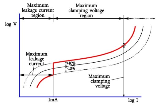
Practical, standard-based limits for the varistor are shown in Figure R5-29.
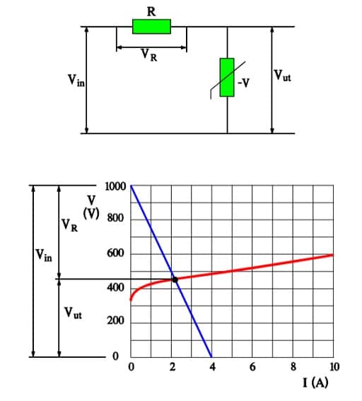
R 5.3.4 Principles of voltage limitation
If the varistor is to operate as a voltage limiter a series impedance is required in the circuit. Common straight conductors have both resistance and inductance (≈ 1nH/mm) and provide in themselves a certain protection. Practically, however, the problem is solved by a series resistor of some hundred(s) of ohms (Figure R5-30).
R 5.3.5 Response time
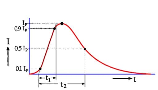
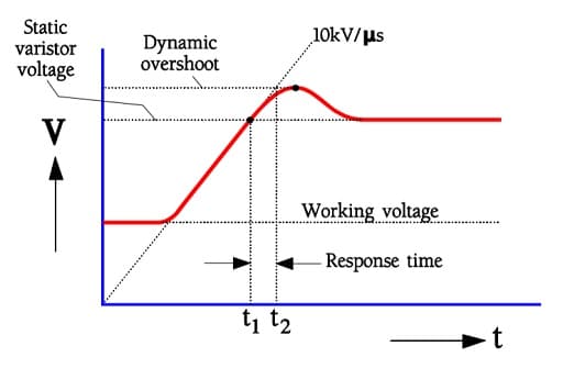
When a varistor is struck by a voltage transient the voltage rises across the component until the cutting characteristics start. There is, however, a short delay, a dynamic effect, that produces a certain overshoot, according to Figure R5-31. As an example there is shown an incoming pulse with a rise time of 10 kV/µs. The response of the varistor time is specified as the rise time t2 – t1 in the figure. The response time seldom exceeds 20 ns; response time of multilayer varistor SMDs usually is less than 1 ns. The response time sometimes is called turn on time.
R 5.3.6 Choice of type
Choosing the correct varistor presupposes a thorough determination of working voltage, including tolerances, expected transients, their duration, pulse energy and repetition frequency. In addition we have to take into consideration environmental requirements and mounting conditions. Connecting two varistors in parallel in order to increase the current load capability should be done only if the varistor voltages (at 1 mA) differ from each other by less than 1 %. Otherwise the unbalance of the load may be considerable and in the most unfortunate cases amounts to 1000:1.
R 5.3.7 Failure modes
The most common failure mode is short-circuiting which may occur after unacceptably high and energy rich voltage pulses or after operation at a steady-state voltage beyond the voltage rating. In the latter case the failure mode might change into open-circuit due to melting effects in the terminal joints or rupture of the package when the large amount of energy generated causes expulsion of the package material.
R 5.3.8 Reliability
The reliability of non-linear resistors, including varistors, is today regarded as relatively good. Not least it depends on serious manufacturers using SPC based production programs and having verified type approvals. Examples of climatic category classified products 40/125/56 are other indications of a good quality. Furthermore, if we choose glass/metal packages the quality will be even better.
Nuclear radiation
Tests with radioactive radiation in the form of neutron, β and γ radiation show that varistors are capable of withstanding high intensities without any effects on the characteristics.
* Occurring capacitance leads to a capacitive shunting that makes the varistor unusable at higher frequencies.
Application
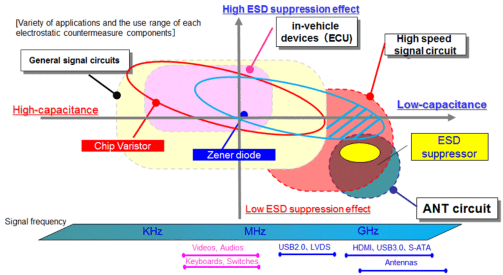
Multilayer SMD varistors are used mostly to protect electronic devices from electrostatic discharge (ESD).
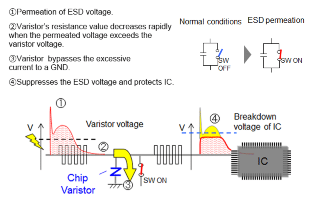
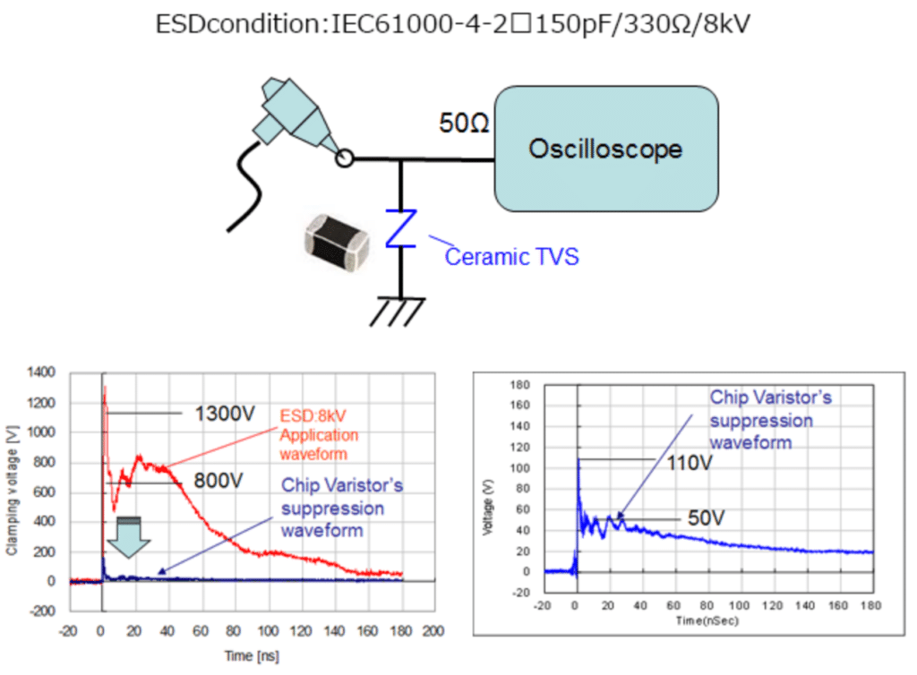
ESD protection benchmarking