Ceramic Capacitors Construction and Manufacturing Process
Construction of ceramic capacitors was already explained in the referenced articles – just in summary – we have two basic types of ceramic capacitor designs
Single layer ceramic capacitor SLCC
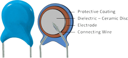
- simple construction
- low cost technology
- lower CV
- higher ESR
- wide voltage range
- high voltage, high power applications
- RF/microwave applications
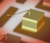
Multilayer MLCC ceramic capacitors
- mass volume
- miniaturization
- low ESR
- high CV
- flexible technology
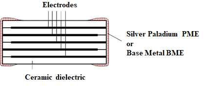
Manufacturing Process – MLCC
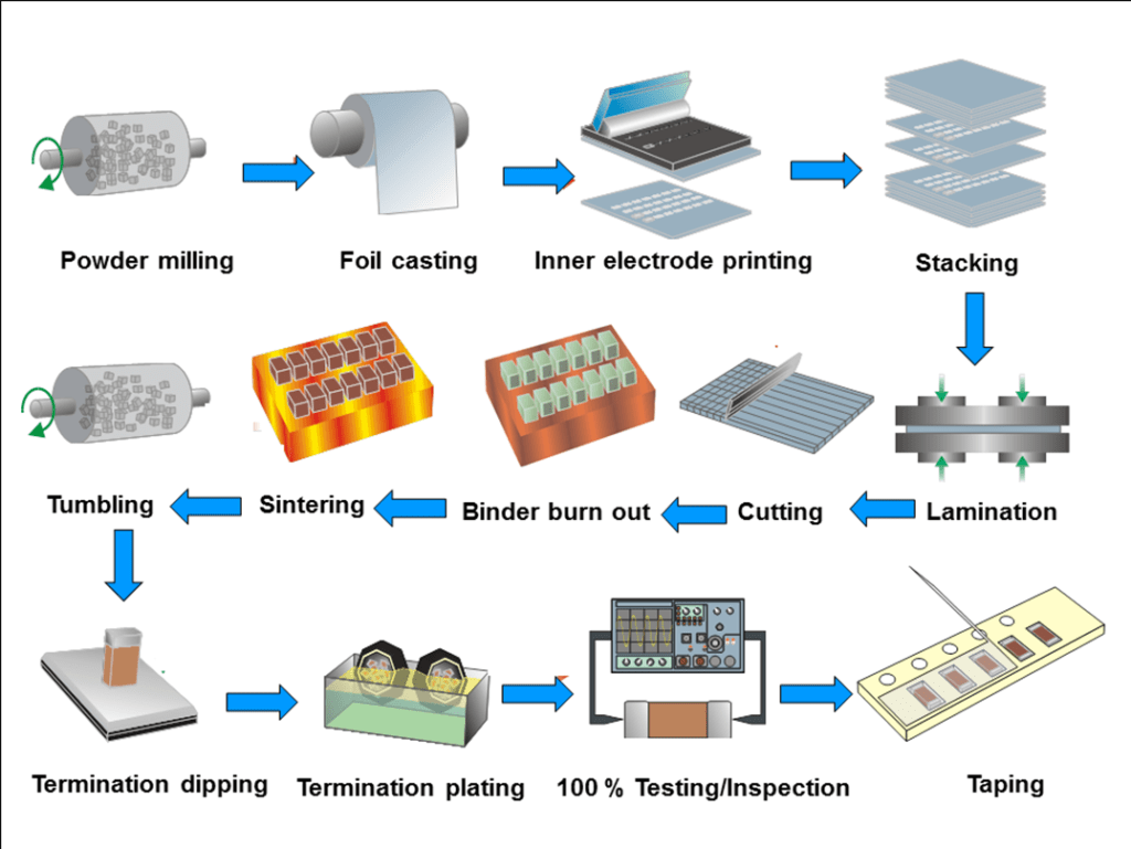
An MLCC consists of a number of individual capacitors stacked together in parallel and contacted via the terminal surfaces. The starting material for all MLCC chips is a mixture of finely ground granules of paraelectric, ferroelectric or anti-ferroelectric raw materials, modified by accurately determined additives. These powdered materials are mixed homogeneously. The composition of the mixture and the size of the powder particles, as small as 10 nm, reflect the manufacturer’s expertise.
A thin ceramic foil is cast from a suspension of the powder with a suitable binder. This foil is rolled up for transport. Unrolled again, it is cut into equal-sized sheets, which are screen printed with a metal paste. These sheets become the electrodes. In an automated process, these sheets are stacked in the required number of layers and solidified by pressure. Besides the relative permittivity, the size and number of layers determines the later capacitance value. The electrodes are stacked in an alternating arrangement slightly offset from the adjoining layers so that they each can later be connected on the offset side, one left, one right. The layered stack is pressed and then cut into individual components. High mechanical precision is required, for example, to produce a 500 or more layer stack of size “0201” (0.5 mm × 0.3 mm).
After cutting, the binder is burnt out of the stack. This is followed by sintering at temperatures between 1,200 and 1,450 °C producing the final, mainly crystalline, structure. This burning process creates the desired dielectric properties. Burning is followed by cleaning and then metallization of both end surfaces. Through the metallization, the ends and the inner electrodes are connected in parallel and the capacitor gets its terminals. Finally a 100% measuring of the electrical values will be done and the taping for automated processing in a manufacturing device are performed.