
Construction of Electrostatic Capacitors
Lets start with a general consideration of electrostatic capacitor designs. There are some design solutions and “tricks” to reinforce capacitor features to meet specific application requirements such as higher power, higher safety robustness.
C2.0 ELECTROSTATIC NON-POLARIZED CAPACITORS
C2.1 CONSTRUCTIONAL SOLUTIONS
The search for capacitance in small volumes has created a number of different solutions, each with its advantages and drawbacks. We shall try in this chapter to describe both methods and problems of achieving large C/V ratios. Further details may be added in specific material sections.
The latter part of this chapter deals with some general construction questions.
C 2.1.1 Stacking
Suppose we have 6 capacitor elements consisting of 2×6 electrodes organized as in Figure C2-1. We understand that spread in one plane and connected together they will result in a total capacitance 6 C. Generally, N electrodes give the capacitance N/2 C.
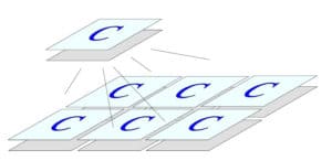
Instead, if we stack them according to Figure C2-2 capacitance will be developed between every electrode with different polarity which here results in 12-1 = 11 elements connected in parallel. Ctot = 11C. In general N electrodes give Ctot = (N-1)C. The higher N the closer to a doubling of the one-plane capacitance with the stacked capacitor type.
C 2.1.2 Winding
If we spread two metal foils separated by two insulating foils as shown in Figure C2-3 (a) and wind the foil package to a winding (b) the capacitance is doubled in the same way as with the stacked type. The electrodes will be capacitive in two directions (c).
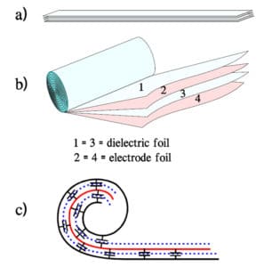
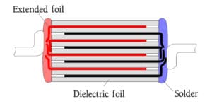
Terminations

The termination to the electrodes is performed either with one or several so called inserting tabs (for example tinned copper foils) which connect the electrodes with the terminals). Or one can let the electrode foils extend from the winding and bend them against the winding end (extended foil construction) where they are soldered or welded to the terminal leads (Figure C2-4). A remark concerning inserted tabs. Should the working voltage be low and the capacitor oil impregnated the tabs have to be welded to the electrode foils if we shall avoid open circuit risks. In electrolytics aluminum tabs have to be welded – preferably cold welded – to the foils because of the corrosion risk.
C 2.1.3 Surface magnification
An important method to increase the capacitance amounts to magnifying the active electrode surface by etching or sintered powder technology. But these technologies are applied only with electrolytic capacitors – short-name ”electrolytics”. We shall revisit this subject later.
C 2.1.4 Minimized electrode spacing
In accordance with the formula C = ε x A/d we improve capacitance by the degree to which we decrease the electrode spacing, d. Improved technology has permitted manufacture of certain plastic films down to less than 0.5 μm (0.02 mils) in thickness. The so called wet method used in ceramic manufacturing has lead to thicknesses less than 15 μm (0.6 mils) and a developed dry method based on a plastic film conveyor or carrier has reduced the dielectric thickness even further, to less than 5 μm (0.2 mils). (The very important production of dielectrics by oxidizing in electrolytic baths will be dealt with in the chapter ”electrolytics”).
To the thinnest dielectric of different material groups corresponds the lowest rated voltage capability. We have to comply with that thickness irrespective of the working voltage. If we, for example, need 6 V DC the nearest working voltage might be 10 V. But only in ceramic. Plastic films stop at 16 V, porcelain and paper at 100 V, mica at 125 and glass at 250 V DC.
The dielectric withstanding voltage
puts another limit to the thinness of a dielectric. The higher the working voltage, the thicker the dielectric must be. But if the thickness increases 5 times, the capacitance decreases to 1/5 or for the same capacitance, the volume of the part must be 5 times greater. Hence high voltage capacitors always will be bulky.
C 2.1.5 Higher dielectric constant, εr
Plastic and paper foils have a relative dielectric constant around 3. If we change to ceramics it’s possible to increase the εr by several thousands. But in different ways we loose the quality characteristics significant for other materials, such as, polymers. In the different dielectric material groups we will account for the typical characteristics.
C 2.1.6 Metallizing
The so called foil capacitor has electrodes consisting of aluminum, 5…10 μm (0.2…0.4 mils) thick. Every turn in a capacitor winding adds at least 2×5 μm (2×0.2 mils) metal foil + dielectric which means that the electrodes in a low voltage capacitor accounts for the greater part of the volume. By means of metal vaporization in vacuum – the so called metallization – the foil electrodes are replaced with a very thin metal layer on one side of the dielectric foils. On metallized paper foils (MP) the metal usually is zinc (Zn). Its sensitivity to oxidation and corrosion in moisture is overcome by the necessary impregnation of the paper winding. In plastic foil capacitors generally no impregnation is needed and here one has been obliged to use aluminum (Al) because of its better chemical resistance. Now, however, some corrosion resistant alloys are introduced with the same advantageous characteristics as zinc.
The metallization layer is thinner than 0.1 μm with typical values around 0.02 to 0.05 μm (0.8 to 2 microinches). The specific capacitance gain is considerable.
The vaporized metal is at a high temperature and therefore the dielectric foils have to be cooled down significantly in order not to be damaged. This is achieved by letting the foil pass over drums cooled down to -30°C in the metallization chamber. The surface texture of the film certainly is changed but otherwise it is preserved intact. Some non-polar plastics like polypropylene (PP) initially suffered from problems with the adhesion to the metal. Currently manufacturers have learned to pre-treat the plastic surface properly.
In some constructions the metal foil electrodes are re-placed by double-sided metallized plastic foils, usually polyester. The design has a number of advantages, not only compared to metal foil electrodes.

Advantages to double-sided metallizing.
- Plastic foils can be made thinner than metal foils.
- TC of certain materials is unfavorably affected by the mechanical forces in metal foils.
- Metal foils also may produce capacitance hysteresis at temperature changes.
- The double metallizing increases the pulse load capability significantly compared to single metallized designs.
- Finally the metallization permits self-healing breakdowns. Because of reduced charge current densities the metallization could be correspondingly thinner, thus reducing the required self-healing energy.
Drawback.
- The voltage rise time/pulse capability is not of the same magnitude as that of metal foil designs.
Termination
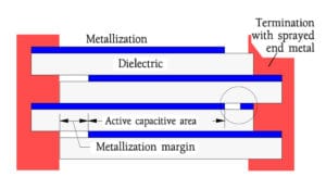
The metallized layer is connected to the terminals by means of a sprayed metal compound applied on the winding or stack ends. The process sometimes is called schooping. By shifting the foils alternately and terminating their metallization a little bit from the edge a short circuiting to the opposite terminal is prevented (Figure C2-6). The figure also shows the active capacitive area which for obvious reasons is maximized. It is done at the expense of the metallizing margins. The balance between security against short circuit and as small margins as possible requires great skillfulness and manufacturing accuracy. Margins of 0.2…0.3 mm (8…12 mils) are regarded as risky with respect to the IR quality while a margin of 1 mm (40 mils) eliminates these risks. Some manufacturers metallize the whole width of the foil and make a laser cut along one edge – encircled area in Figure C2-6 – and achieve in this way a more controlled metallizing margin simultaneously as they obstruct forbidden penetration of the end spray metal. Note however that the figure following, for reasons of emphasis, is far from being to scale.
The termination quality varies from one manufacturer to another. Therefore it is of vital importance by simple means to be able to detect parts with fault terminations. The utilization of ESR measurements taken at the resonance frequency of the capacitor in order to evaluate the contact quality in metallized film capacitors successfully has been used by number of companies in practice. For example, if the test specimens have been subjected to a heat treatment the differences in ESR quality appear most distinct.
Voltage rise time / current pulse
Because the metallization is very thin and its connection with the end spray metal is a surface contact and not a bulk metal layer the current into the electrodes must be limited. Above all, it is pulse loads that are the problem. When the charges rush in from the ends they successively are bound to the electrodes. Hence the highest current densities are at the electrode edges. Exactly here there is a risk that the ESR of the contact junction causes a local rise in energy development that a weak spot in the metallization is burnt off. This burning reduces the remaining current area. The next current pulse will result in an incrementally higher current density over the remaining area, the next weakest spot is burned away, and so on. Eventually the part fails open. The current, which can be described as dQ/dt, depends with start from the formula C1-1 of the voltage differential quotient as
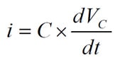
…….. [C2-1]
Therefore metallized film capacitors must not be subjected to more than the limited voltage differential quotients that the manufacturer states in his data sheets. Here are some examples of stated maximum values:
- standard capacitors 5…20 V/μs.
- pulse application types 100…2500 V/μs.
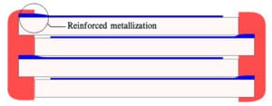
In pulse applications the weakest link in the current paths is reinforced, i.e. the joints between end spray metal and the metallized layer. Among other means, reinforcement is achieved through choice of a suitable end spray metal, by reinforcement of the metallization along the contact edge as shown in Figure C2-7 and more and more often by contact favorable metallizing alloys. Some stacked types (see next passage) with Al metallization have an end spray of aluminum. Also the double-metallized electrodes as already described under 2.1.6 represent a considerable improvement of the pulse capability.
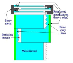
A further improvement of the pulse strength is a combination of the reinforced metallization and a wavy cut in the foils as shown in Figure C2-8. The wavy cut enlarges the contact area which means a lower contact resistance and a subsequent higher pulse strength.
Metallized stacked capacitors
If a winding should experience repeated voltage or current pulses that start burning off marginal parts of the contact edge it will, according to our previous discussion, end up with a complete open circuit. If instead of a winding we had had a stack of metallized foil parts (stacked type) an element with a degraded contact should have been eliminated. But the current into the remaining elements won’t be changed because one element is burnt off. The capacitor will work equally well at repeated pulses (with somewhat reduced total capacitance). The safety margins against contact edges being burnt off can, for stacked capacitors, be reduced which means the pulse rating can be kept higher in comparison to the rating for a corresponding wound design.
The manufacturing is done so that one winds a so called mother capacitor on an enormous wheel. The mother capacitor is metal sprayed (schooped) from the sides and then segmented to form capacitors which are finally finished in the usual way. The large diameter of the mother capacitor makes every little sector piece (part capacitor) nearly planar. When the saw cuts through the mother capacitor the plastic melts in a surface region and fragments of the metallization are dispersed in the locally melted plastic so that a sufficient insulation distance is created between the electrodes. In another method of manufacturing one winds on a flat plate and cuts the large plane parts of the winding into suitable elements.
Self-healing
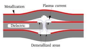
Dielectrics always have weak spots or defects and thinner zones which are more sensitive to breakdowns than the ordinary material. A breakdown, i.e. a short circuit through the dielectric, leads to local energy generation which transforms the material in the breakthrough canal into a plasma and vaporizes the thin metallization around the breakthrough hole. Around this hole with a diameter of 5…100 μm (0.2…4 mils) there is created a metal-free insulation area approximately 0.1 to 3 mm (4 to 120 mils) in diameter. The instantaneous short circuit thus is turned into an open circuit. The phenomenon is called self-healing (Figure C2-9). The condition for self-healing is a certain minimum energy estimated to be at least 10 μJ. Small part capacitances or low working voltages, therefore, may lead to a lack of self-healing if a breakthrough nevertheless should occur in a weak spot, e.g. under extreme heat when the dielectric has grown weaker.
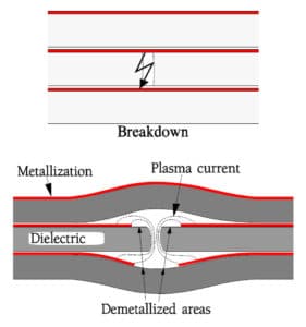
As indicated in Figure C2-9 the self-healing energy creates a plasma. Its temperature and pressure are extremely high but with short duration. The gas pressure developed around the breakthrough site propagates and separates the adjacent dielectric layers to an extent while the decomposition products are spread over the surrounding metallization and plasma pressure and temperature drop. The whole series of events for typical energies occurs within 0.01 to 1 μs. Electrically, the event manifests itself in an abrupt voltage drop which is restored as a charging curve, usually within 100 μs. The time constant is determined by RC product of the immediate external circuit. It’s a rare occasion that the whole existing energy is used for the self-healing. The voltage drop usually don’t get any further than
- a few to some tens % of the total load voltage in metallized plastic film capacitors and
- 10 mV…1 V in MPs (metallized paper) and lacquer film capacitors ( cellulose acetate).
The self-healing design permits lower safety margins between the breakdown voltage and the rated. A short circuit doesn’t have to be avoided at any price. The ratio of breakdown voltage to rated voltage can be decreased from (10…15):1 to (3…6):1 which reduces the thickness of the dielectric foils correspondingly.
Resulting effects of a self-healing
During self-healing the polymeric dielectric is decomposed. Carbon-rich compounds generate amorphous carbon which will be deposited on cavity walls and, unfortunately, also on the insulated burned off surfaces around the breakthrough hole and its canal walls (Figure C2-10).
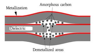
Compounds very rich in carbon, such as polystyrene, generate so much carbon that they are impossible to use in a customarily metallized design. The carbon deposits destroy the IR after a self-healing.
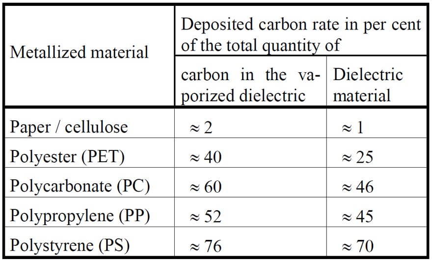
Other materials have a varying degree of carbon generation (Table C2-1). That information, however, must be combined with information on the clearing chemistry of the materials. Best is PP followed by PET and the poorer PPS and PEN.
Even if the deposited graphite does not destroy the IR, sometimes graphite particles under the influence of weak field strengths line up to form conductive strings with an unstable resistance in the range of some hundreds to some hundred kΩ. In practice this is a short circuit. If the voltage is raised or the circuit impedance doesn’t limit the current the conductive carbon string is burnt off. We never experience the phenomenon in practice because the required energy is much smaller than that of a self-healing. If the application, however, is critical and works in high impedance circuits at temporarily low field strengths the short circuit doesn’t disappear. Hence, certain dielectrics in film capacitors should be avoided if we don’t purchase capacitors after they have passed extensive burn-in and powered thermal cycling testing.
The risk of this type of carbon deposits increases with the internal pressure of the winding. Precision capacitors are, for example, wound on a core with a relatively high tensile stress which gives a dense and mechanically stable winding. The following figure shows schematically the approximate internal pressure distribution in some different winding types.
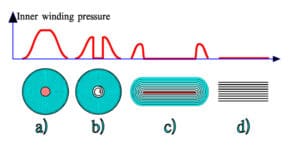
- a) winding on a core,
- b) winding without a core,
- c) flattened winding,
- d) stacked-type.
In severe cases the winding pressure may approach 100 bars (» 1450 psi). But the internal pressure prevents the plasma from expanding with the consequence that the carbon deposit is concentrated at the immediate breakdown site. This in turn increases the risk of ”carbon string” short circuits. Furthermore, the risk of damage to neighboring dielectric layers increases if the developed energy corresponds to high working voltages (Figure C2-12).
In the most severe case self-healing under these conditions results in a thermal run-away where the capacitor is destroyed and may burn.
Flattened windings
Windings not wound on a core will become loose in its center where the removed shaft has been but will achieve a relatively high pressure further on into the winding. If such windings are flat the part will have two advantages. First the center will become more rigid. Second the long sides of the flat cross-section will facilitate expansion if there should be any self-healing (Figure C2-11).
C 2.1.7 Heat treatment / shrinking
The body stiffening which is created by metal foil electrodes disappears with the use of metallized foil electrodes. The winding becomes looser and is more readily subject to the formation of creases and cavities. If it is not impregnated the risk of corona increases in alternating voltage applications. To some extent, however, these drawbacks can be eliminated in plastic film capacitors, metallized as well as foil electrode types. The used plastic foils are cold-rolled both lengthwise and to some extent also in breadth in order to achieve a thinner foil. New technologies giving better film properties use a simultaneous biaxial stretching to get the wanted film thickness. Anyhow, the molecules are ”frozen” in a compulsory position. But at a certain elevated temperature they start leaving this position. At a continuous temperature rise the process eventually ends up with all molecules retaining their initial position completely. This occurs through baking the winding at certain elevated temperature. The winding shrinks slightly and becomes harder. But the temperature rise must be limited. Otherwise the shrinking will continue which in turn may cause deteriorated joints between end spray and metallization, increasing losses (ESR) and loss of capacitance. The development of surface mount (SM) types that can endure soldering heat therefore has encountered many problems. Two principal approaches are distinguishable. One is utilizing the encapsulation as a heat shield, the other erases the molecular memory of their position before the cold-rolled stretching.
Which approach is preferable may depend on utilized soldering process. Independent of line, type and manufacture it’s advisable to evaluate the quality of parts before and after soldering. According to the authors opinion the best way is by measuring the ESR at the resonance frequency. See C 2.1.6, Termination.
C 2.1.8 Impregnation / Voltage distribution
Capacitors that must operate at voltages where corona effects start to appear must not contain gas or air filled cavities. As shown in section C1.2.3, example from Figure C1-15, the electric field strength in the void was several times higher than in the homogeneous dielectric. Hence, cavities which can’t be avoided through good manufacturing technology have to be eliminated in some way or another.
One way of elimination of cavities is with impregnation (an absolute necessity if paper windings are used). Mineral and silicone oils, waxes and epoxy are the most common impregnants. Currently, as they fill internal cavities and increases the tension stability they also influence the dielectric constant slightly.
The impregnation is performed in vacuum in order to fill all cavities completely. It’s not that easy – one could do with various means available in order to succeed perfectly – and here the liquid impregnation agents are advantageous. However, mineral oils should not be used with metallized foil capacitors because the self-healing action decomposes and contaminates the oil whose insulation resistance (IR) then decreases. Instead, some vegetable oils are used.
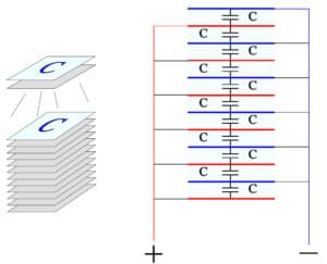
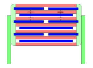
Even if we have succeeded perfectly with the impregnation and kept the electric field strength in the dielectric within permitted limits by increasing foil thickness, there are limits for the operating voltage. Along the edges of the electrodes field strengths are developed that at a certain magnitude cause a flash-over. Thus one is forced to distribute the voltage over several capacitor elements. For non-impregnated capacitors this construction solution must be engaged even sooner because of the corona risk. The principle is shown in Figure C2-13 where the elements are connected in series through a common ”free-standing” foil. The electrodes consist of real metal foils or one or double sided metallized plastic films or a combination of these types.
In principle, with this type of connection, we exchange parallel electrodes for series connected ones. While the voltage capability is doubled in the same capacitor volume the capacitance is reduced to one quarter, quite in accordance with the formulas C1-4 and C1-5.
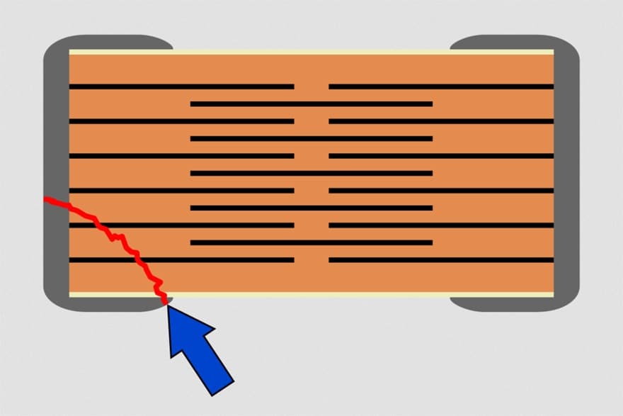
Such design with “floated” electrodes is also used by ceramic capacitor safe design to suppress critical crack issues – see figure on right.
C 2.1.9 Hermetic encapsulation
Sometimes components need encapsulations that are moisture barriers. Then, no lacquer or polymeric seal, however good, will do. Humidity will diffuse through such materials with sufficient time. In this application only certain inorganic materials as glass, metal and solder will do. A common combination is metal cans with glass and solder seals around the terminal leads. We shall not enter upon all those problems one then has to consider in order to match glass types, thicknesses, diameters and alloys in the feed-throughs etc. and thus bring about components which will withstand also temperature changes. One failure mode, however, we shall consider. It occasionally occurs with hermetic components having a solder seal around the terminal leads. Figure C2-14 represent such a typical component with metal bushings and solder seals.
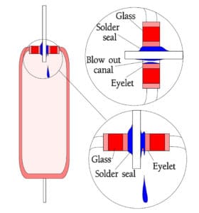
The solder sealing usually is made with the can in a perpendicular position which may result in a risk of melted solder dripping into the can, especially if the other feed-through is not yet sealed so it can create a ”back-pressure” from the gas inclusion which will prevent the solder from dripping. Later these solder beads or droplets may cause short circuits, especially in components with insertion tabs. In addition the internal gas pressure in the can may cause failures. If the sealing process conveys too much heat before the solder has solidified there is a risk that the pressure may open a tiny duct in the solder seal (a so called blow-out). Such an internal gas pressure may be produced also during the soldering process. If the solderability is poor a prolonged soldering process may cause conditions for a blow-out. This failure mechanism has been observed in solid tantalum capacitors.
Hermetic components with solder seals often comply with US and other MIL standards. Even if such components meet these MIL spec standards it must not be assumed that there are no loose solder beads inside the components. Such a quality level is guaranteed to a degree if real-time or micro-focus X-ray control is included in the manufacture inspection.
C 2.1.10 Epoxy sealed casings
It is usual to mold epoxy around components in metal cans or plastic casings. It is then important both that the box compound has been degassed first and that the filling operation takes place in a low pressure chamber so that the epoxy really penetrates into and surrounds the body and prevents forming of cavities and gas bubbles. Otherwise there will be places where diffusing humidity can condense if there is a sufficient decrease in temperature and cause problems. The risk is especially large when a cylindrical metal can is sealed from one end with epoxy. We know of one instance where a component style that had performed very well in a 56 day humidity test as specified in IEC 68. A 48°C freon washing and a subsequent rinse in distilled water of room temperature created such great temperature differences between the metal can and epoxy molding that the adhesion yielded. A slit opened along the metal wall and in those unfortunate cases where cavities occurred in the bottom of the can – Figure C2-15 – there the negative pressure in the cavity sucked in washing water that hit the exposed porous spray metal. Its capillary forces then transferred the water to the metallized electrodes and thus created a perfect electrolytic cell. Within a few hours electrolysis consumed most of the metallizing.
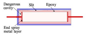
This same type of capacitance decrease has been observed also in metallized plastic film capacitors with radial leads in plastic casings. In a batch with an anomalous epoxy filling there were deep cracks down to occurring cavities localized against the end spray metal on the winding. Washing water mixed with flux then was sucked into the cavities, resulting in the same failure mechanism.
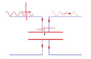
C 2.1.11 Four terminals
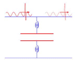
Assume now that a transient enters the circuit shown in Figure C4-16. Because the conventional lead mount decoupling capacitor has a certain inductance in the leads – approximately 1nH/mm lead length – the entrance is blocked for the transient that proceeds further towards the load.
In order to remedy the problem so called four terminal components are used, where both the signal and the transient are forced towards the capacitor electrodes (Figure C2-17). We can see also the similar princip in three terminal devices where, one termination is conventional and the other is split into two.
Note that the more and more common chip components in principle have the same type of noise suppressing termination as that of the four terminals.
C 2.1.12 Flammability
Components which run the risk of meeting with overvoltages that can lead to short-circuits, especially so called X and Y capacitors, they must be able to withstand certain flammability tests without being set on fire or burn. One distinguishes between active and passive flammability.
With passive flammability is understood the property of a component to continue burning after external ignition, i.e. ignition caused by energy applied from the outside of the component. Reference IEC 695-2-2.
With active flammability is understood a spontaneous ignition without external ignition.
Passive flammability can be brought about by self-extinguishing materials in casings and impregnation. Above all the resin impregnated metallized paper capacitor(MP) has a clear advantage over the metallized plastic film capacitors.