
Class I Ceramic Capacitors
C 2.10 Ceramic Capacitors Class I
Capacitors with Class 1 ceramic are manufactured with temperature coefficients between +100 and –1500 ppm/°C. In tables and diagrams we will confine ourselves to the type that is called NP0 or COG (0 ± 30 ppm/°C) and which is predominant over all remaining Class 1 variants.
To the Class 1 ceramics we also count porcelain that above all is found in certain HF chips.
C 2.10.1 General comments to Class 1
The type is characterized by small losses, high IR, high stability, linear and moderate TCs between +100 and – 1500 ppm/°C and an εr between 5 and 450. The tolerances range down to ±1%. Capacitances lower than 10 pF are difficult to produce to a percentage accuracy. The tolerances are rather stated in absolute values: ±0.1pF, ±0.25pF, ±0.5pF and ±1pF.
At construction and failure analysis you may sometimes find a pit in the ceramic of Class 1 capacitors. It may extend through all layers and is filled with some inert compound, often glaze. It is a so called trim pit where part of the electrode surface is blasted away in order to match the capacitance value towards finer tolerances, for example 1 or 2%.
The ceramic mass shrinks namely strongly during the sintering – approximately 15% – and this may cause the capacitance distribution to get so askew that it will be necessary to adjust it by trimming. The trim pits are harmless provided the filling compound don’t contain any blisters at the edge to adjacent layers.
The small losses in Class 1 ceramics do not correspond to a similarly low dielectric absorption. On the contrary it is relatively high, approximately 0.5…1%.
The dielectric consists either by one layer – as a tube or in a plane shape, SLC from Single Layer Ceramics, or by several layers in stacked form, MLC from Multi Layer Ceramics. In MLCs the capacitance range is determined by the number of layers. At minimum it consists of one layer and at maximum it is limited by the manufacturing technique and for economical reasons. The noble metal AgPd paste of the electrodes is expensive, mostly used BME is a cheaper variant.
The temperature coefficient often is denoted by N(egative) or P(ositive) followed by the value in ppm/°C. Here some examples where we within brackets mention also the corresponding EIA designation:
- P100 = +100±30ppm/°C; (EIA = M7G)
- NP0 = 0±30ppm/°C; (EIA = COG)
- N150 = -150±30ppm/°C; (EIA=P2G)
- N1500= -1500±250ppm/°C; (EIA=P3K).
US MIL specifications have other designations.
In diagrams and tables we henceforth confine ourselves to the predominant NP0/COG ceramic.
C 2.10.2 HF chips
When the frequency raises to some hundred MHz conventional ceramics in MLC design starts reacting with high and exponentially increasing losses. We come a step on the way by modifying the ceramic. By passing to porcelain (εr = 12…15), which we include under the concept ceramics Class 1, the losses decreases sharply. Another way to reduce the HF losses is by passing to a single layer design, SLC, and moreover introduce thin film electrodes in gold (Au), copper (Cu) or aluminum (Al). As a dielectric silicon dioxide (εr = 4.4) or silicon nitride εr = 7.5) is used.
Sometimes a changeover to mica capacitor chip can reduce the losses.
The losses in HF capacitors sooner are expressed in the quality factor Q (=1/tan δ) than in tan δ.
C 2.10.3 Measurement conditions
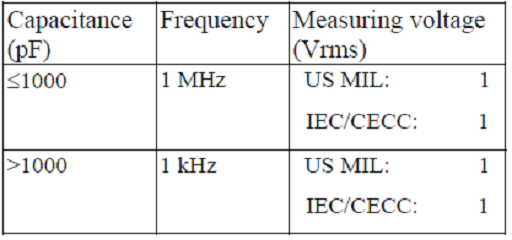
Table C2-8. Measurement conditions Class 1 ceramics.
At IR and voltage strength tests sometimes in MIL and IEC/CECC a charge and discharge limitation of maximum 50 mA is specified. Comments: These limitations probably are based on older manufacturing technologies. Some manufacturers nowadays have chosen to delete these requirements in their catalogue sheets. Corresponding voltage rise times will for capacitances above 1 nF be unrealistically low. Such capacitors manage according to performed tests as a rule at least 100 to 1000 times higher inrush currents, even at repetition frequencies in the kHz range.
Diagrams
As usual we shall present a number of diagrams describing the different characteristics versus temperature and frequency.
C 2.10.4 Temperature dependencies
Capacitance and Tan δ versus temperature
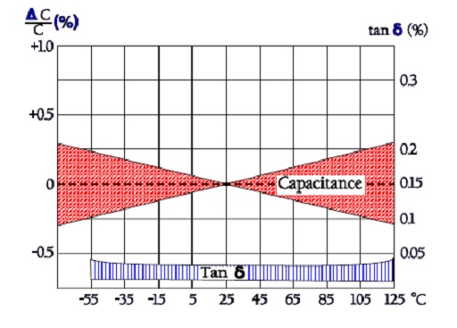
Figure C2-77. Capacitance and Tan δ versus temperature. Typical curve ranges for NP0/COG.
IR versus temperature
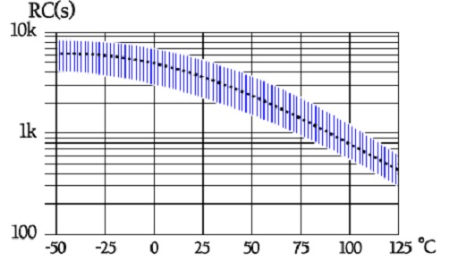
Figure C2-78. Typical curve range for IR versus temperature in Class 1 ceramics.
Comments to Figure C2-78 about RC product and IR.
When we convert the RC product to insulation resistance (IR) expressed in MΩ and go down in capacitance the IR increases correspondingly. Specifications usually set limits to the IR increase at 10 nF. Ac-cording to the typical curve in the figure RC is approximately 4000 s at 25°C which gives an IR = 4000/10(nF) = 400 GΩ. Larger values can not be expected for capacitances lower than 10 nF.
C 2.10.5 Frequency dependencies
Capacitance and Tan δ versus frequency
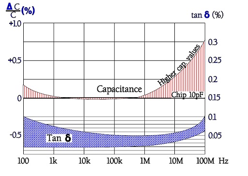
Figure C2-79. Capacitance and Tan δ versus frequency. Typical curve range for NP0/COG.
Q versus frequency
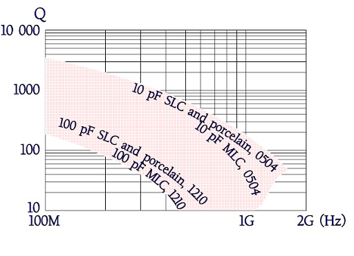
Figure C2-80. Information about Q value versus frequency for chips in porcelain and ceramic.
Notice how the Q value increases with decreasing capacitance and chip size. The figures C2-80 and 82 show examples of the same phenomenon.

Figure C2-81. Example of Q value versus frequency.
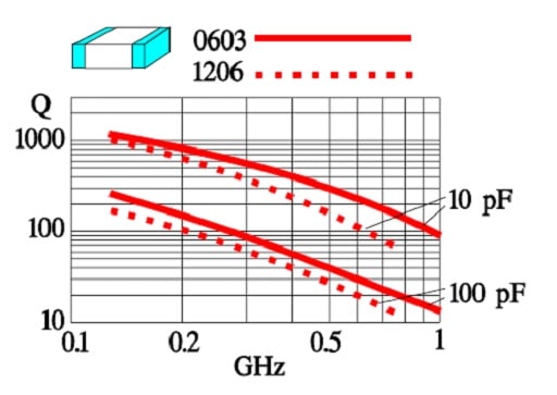
Figure C2-82. Another example of Q value versus frequency and chip size.
ESR for the same chip as in Figure C2-82 is shown in Figure C2-83. Other examples of the frequency dependence of ESR are found in C2-84 to -86.
ESR versus frequency

Figure C2-83. Examples of the ESR versus frequency.

Figure C2-84. Another example of the ESR for 1 and 10 pF.

FigureC2-85. ESR examples for 10 pF and 10 nF.

Figure C2-86. Examples of ESR and impedance versus frequency in a chip and a lead mounted 1 nF capacitor.
Resonance frequency versus capacitance
Examples of series resonance frequency versus capacitance for two sizes of HF chips in MLC design are shown below.

Figure C2-87. Examples of series resonance frequencies for HF chips in MLC technique.
As a comparison to the MLC example above Figure C2-88 shows how a SLC chip in approximately the same size as 0603 may behave.

Figure C2-88. Example of the resonance frequency in a SLC chip.
C 2.10.6 Failure modes
In addition to those failure types presented under C2.9.2 we will mention the following which concerns lead mount components only and AgPd terminations. The termination paste that has to be burnt to the ceramic end faces contains except for silver (Ag) and palladium (Pd) also minute glass granules which at firing combine with the ceramic and bind the Ag-Pd metallizing to the surface. To the metallizing then leads are soldered – see Figure of principle C2-76 – usually in one step.
These end faces, however, sometimes are very small – mm2 if the chips belong to sizes 1805 and 1808 – and this raises high claims for the quality of the silver layer, for the melting time and solder temperatures during the soldering. If the silver for some reason comes loose from the ceramic it’s not sure that the failure will be detected during the manufacture though this failure type strikes parts of whole manufacturing batches.
The capacitor elements are namely encapsulated in some thermoset plastic or thermoplastic resin which locks the leads in their position. Usually a slight pulling in the leads to suspect batches during capacitance measurements will do for revealing the failure in at least some samples. The failure, that is quite exceptional, is methodical and accordingly strikes whole manufacturing batches.
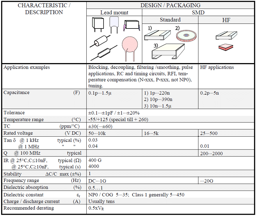
Table C2-9 CERAMICS CLASS 1 / NP0 / COG