
Class II Ceramic Capacitors
C 2.11 CERAMIC CAPACITORS CLASS 2
Ceramic Class 2 capacitors can be divided in two main groups, one with a moderate temperature dependence for the class – ΔC ≤ ±15% within the temperature range – and the other with such changes that only a fraction of the capacitance remains at the temperature limits. The first group is in our tables and diagrams represented by the ceramic type denominated X7R or 2C1, the latter by Z5U or 2F4.
C 2.11.1 Introduction to Class 2
Class 2 capacitors are characterized by high dielectric constants, often designated with a K followed by the εr. Hence K2000 means εr ≈ 2000. The temperature dependence of the capacitance is large. Therefore EIA characterizes the ceramic with three characters that in order state the lower and the upper limit of the temperature range and last the capacitance change within the range.
| Letter code low temperature | Number code upper temperature | Letter code change of capacitance over the temperature range |
| X = −55 °C (−67 °F) | 4 = +65 °C (+149 °F) | P = ±10% |
| Y = −30 °C (−22 °F) | 5 = +85 °C (+185 °F) | R = ±15% |
| Z = +10 °C (+50 °F) | 6 = +105 °C (+221 °F) | S = ±22% |
| 7 = +125 °C (+257 °F) | T = +22/−33% | |
| 8 = +150 °C (+302 °F) | U = +22/−56% | |
| 9 = +200 °C (+392 °F) | V = +22/−82% |
Table C2-10. EIA codes for temperature limits and capacitance changes, ΔC.
Example: X7R means with EIA designations the temperature range -55/+125 °C where the capacitance change maximum ±15%, provided the DC voltage is zero. The EIA code don’t take into consideration that the Class 2 ceramic react with capacitance reduction to DC voltages.
On the other hand certain other standards do. Here some examples.
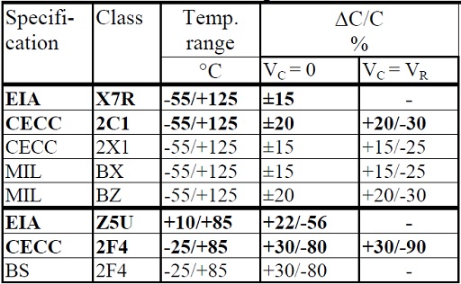
Table C2-11. Comparisons between ceramic classes. ΔC versus temperature and VDC.
Table C2-11 contains two main groups of Class 2 ceramics:
• K900⋅⋅⋅K2200; ΔC approximately ±20% within the temperature range.
• K4000⋅⋅⋅K12 000; very large ΔCs at the temperature limits.
There are within these groups many more materials, for example the recent material Y5V, but in our diagrams and table information we mostly will confine ourselves to X7R/2C1 and Z5U/2F4. By specification Z5U is situated within a more limited temperature range than 2F4 but this has to do only with the specified ΔC, not with its capability to stand up to lower temperatures.
If we can accept the capacitance changes caused by cold the ceramic will stand -55°C. In the diagram section we shall look closer at the temperature dependence of the capacitance. The upper temperature limit, however, should not be exceeded. The capacitance tolerances for X7R usually are ±5, ±10 or ±20%. Usual Z5U tolerances are ±10, ±20 or -20/+80%.
The dielectric absorption is high:
• X7R/2C1 ≈ 2.5⋅⋅⋅4.5%;
• Z5U/2F4 ≈ 4.5⋅⋅⋅8.5%.
C 2.11.2 Measurement conditions
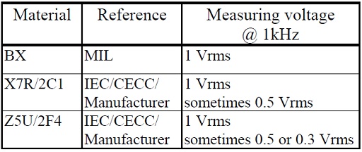
Table C2-12. Class 2 ceramics.
That the measuring voltage is specified and limited depends among other things on the capacitance which changes with applied alternating voltage. See examples in figures C2-89 and –93.
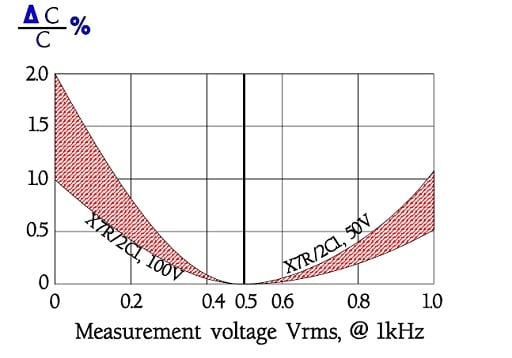
Figure C2-89. Examples of ΔC versus measuring voltage for X7R/2C1 with different rated voltages.
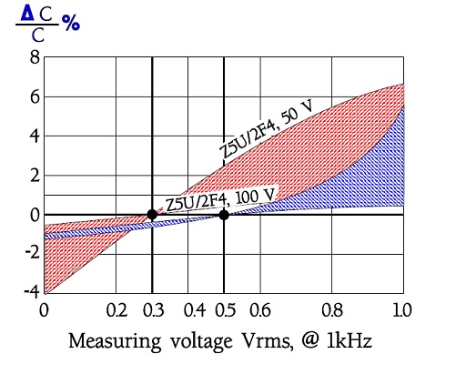
Figure C2-90. Examples of ΔC versus electric tension for Z5U/2F4 with different rated and reference voltages.
C 2.11.3 The Curie temperature
Ceramic capacitors have a crystalline structure and dipoles that give the materials their unique dielectric constants εr. But above a certain brittle transition temperature, the so called Curie temperature, the ceramic loses its dielectric properties. The Curie temperature for Class 2 ceramics usually is situated between 125⋅⋅⋅150 °C. The influences don’t occur at any exact switch temperature but make themselves gradually discernible in the vicinity of the Curie temperature. Thus we should rather talk of the Curie range.
C 2.11.4 The dependence of capacitance on applied voltage
Dielectric absorption (DA) and Ferroelectricity
The different types of Class 2 ceramics are based on barium titanates. Their crystalline structure are constituted by dipoles that at the polarizing present a dielectric hysteresis. With pattern from the hysteresis curve of magnetic materials they are called ferroelectric.
Figure C2-91 shows the capacitor charges versus applied voltage.
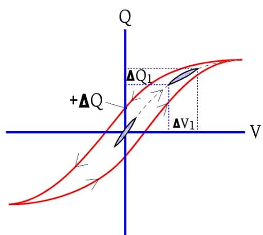
Figure C2-91. Capacitor with ferroelectric hysteresis.
When the voltage increases from zero to a limit value and then decreases, the charging curve follows another branch that at the voltage V = 0 leaves a residual charge + ΔQ. An alternating voltage of the same magnitude will force the charging curve along the outlines of the large hysteresis loop in the figure.
If the alternating voltage is small and the DC voltage = 0, the hysteresis loop will follow the small oval in the center of the figure. Small voltage changes correspond to large charge changes, i.e. to a high capacitance. But if we superimpose a small alternating voltage on a considerable DC voltage we see how ΔV1 corresponds to fainter charge changes ΔQ1. The capacitance has dropped.
Figure C2-91 shows how the ferroelectric material locks a residual charge ΔQ on the electrode surface when the voltage over the capacitor recedes to zero (outer circuit short-circuited). In other words it’s a question of dielectric absorption (DA) according to section C1.1.3, here. But there is a difference, too.
The ferroelectric curve swings to the V axis while the general DA curve looks like a magnified picture of the center oval. In both cases the bound residual charge ΔQ is time dependent. If the outer circuit is short-circuited (V = 0) successively charges on the electrode surfaces are set free while ΔQ decreases.
The ferroelectric energy absorption is polarity dependent. Thus a complete re-polarizing will require more energy than the initial polarizing. But in, for example, D/A converters the pulse time may not be sufficient for a satisfactory re-polarizing.
The considerable dielectric absorption that exists in Class 2 ceramics makes them directly inappropriate for precision integrators like D/A converters, especially if there are positive and negative pulses. The crystalline structure of ferroelectric materials are maintained up to the Curie temperature.
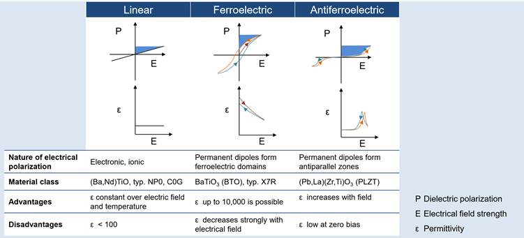
Specific group of materials are anti-ferroelectric dielectrics. In opposite to ferroelectrics, where permittivity decrease with applied voltage, permittivity of anti-ferroelectics is low at low voltage and increase with electric field / appled voltage. These materials can be used to achieve high CV, high capacitance at high voltage applications such as energy generation or EV/HEV vehicles in automotive industry. See figure bellow for comparison of polarisation curves between linear dielectrics (class 1), ferroelectrics (class 2) and anti-ferroelectric materials:
Piezo-electricity
If we expose a Class 2 ceramic material to an electric field strength it will cause faint movements in the ceramic. Inversely a mechanical pressure will create electric charges in the capacitor. The phenomenon is called piezoelectricity. BX ceramics (K900⋅⋅⋅⋅⋅⋅⋅⋅⋅K1800) exposed to chock/vibration produced in an experiment output voltages up to 40 mV3.
If we connect an X7R capacitor to an oscilloscope and bang a hammer on the component we sometimes get high voltage spikes, sometimes not. It depends not only on the way the blow hits but varies from one sample to another. The output voltage is both manufacture and batch dependent.
DC voltage dependence
We showed just with reasoning around the ferroelectric curve how the capacitance decreased with an increasing DC voltage. How the DC voltage influences the capacitance is shown in Figure C2-92. Notice how specification requirements of voltage dependence affect in other respects equivalent materials.
For X7R no requirements are called for – the dependence will be great – , for 2C1 the dependence is maximized to –30%. Within the material classes the voltage dependence increases with the rated voltage. The thickness of the dielectric namely don’t grow in the proportion as the rated voltage. Thus the electric field strength increases with increasing rated voltages which in turn leads to a somewhat enhanced voltage dependence.
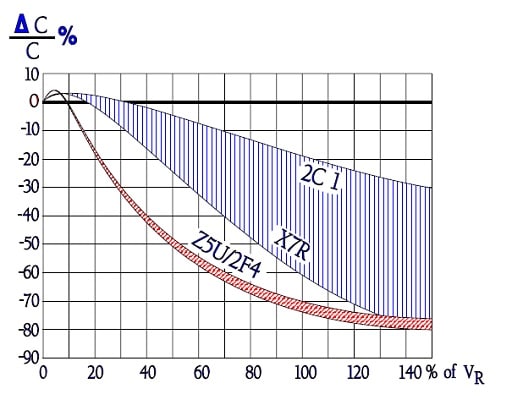
Figure C2-92. Typical curve range for ΔC versus DC voltage in different material classes.
AC voltage dependence
Alternating voltages create a reverse effect than DC voltages on the capacitance.
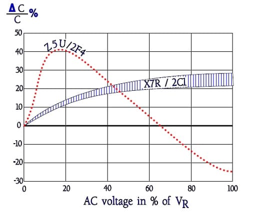
Figure C2-93. Examples of ΔC versus AC voltage in percent of the rated voltage VR.
Let us emphasize that Figure C2-93 represent one example. Great variations may occur. In any case the significance of norms for measurements of capacitance is obvious. At IR measurements and voltage tests MIL and IEC/CECC specify a charge and discharge limitation of maximum 50 mA.
Commentary: The limitations are questionable. Some manufacturers have chosen to delete these requirements in their catalog sheets. Some even specifies voltage rise times of 1000V/μs which for capacitances above 1 nF means surge currents ≥ 1A!
If your application requires considerable charge/discharge currents, please check with the manufacturer – or test for yourself – what the capacitor can stand and restrict the application to single pulses. Class 2 ceramics don’t stand intense periodic pulse load.
C 2.11.5 Aging
Class 2 ceramics lose capacitance with time. The decrease is called aging. It is conformable to a logarithmic law and decreases with a certain per cent per time decade.
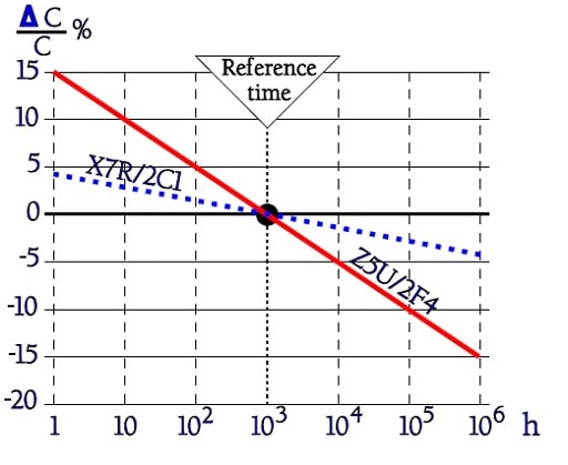
Figure C2-94. Example of aging diagram for X7R and Z5U ceramics.
In the diagram the capacitance of the Z5U ceramic decreases with approximately 6% per time decade and of the X7R ceramic with approximately 1.3%.
Typical aging constants usually are
• BX/X7R/2C1 1⋅⋅⋅2%
• Z5U/2F4 3⋅⋅⋅6%.
The aging constant k, expressed in per cent per time decade, follows the general formula
The capacitance decrease is defined with start 1 hour after cooling. In order to avoid disputes about delivered values relevant norms state that the value shall be guaranteed at the 1000 hrs point. With starting-point from the formula C2-2 the 1000 hrs value then is calculated as
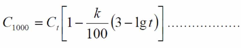
[C2-2]
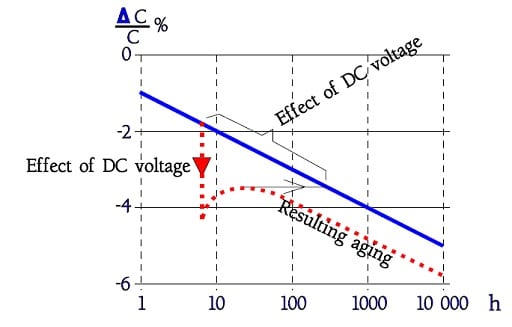
In Table C2-11 it was accounted for the effect of DC voltages. If a temporary DC voltage in the magnitude of VR is applied there will be a lingering effect in the form of a capacitance decrease more or less as if the component had been aged for 1⋅⋅⋅1½ time decade (Figure C2-95).
Figure C2-95. Aging effect from a momentary DC voltage in the magnitude of VR.
In the figure we also see how the capacitance value increases to some extent when the DC voltage – here approximately VR – is removed.
The increase can amount to approximately
• +2.5% for C21 ceramics
• +5% for X7R and Z5U ceramics.
The aging starts by definition 1 hour after cooling. Now if we heat a capacitor above the Curie point and let it cool, the crystal structures orientate themselves in the same way as after the manufacture and the capacitance resume its initial value before it, again, starts subsiding in accordance with the aging curve. One talks of “de-aging”.
Mind that every soldering of chip ceramics result in a deaging. De-aging effects may be evoked already in the lower part of the Curie range if the distance to the Curie point is compensated by a corresponding increase in time.
C 2.11.6 Temperature dependence
Capacitance versus temperature and voltage
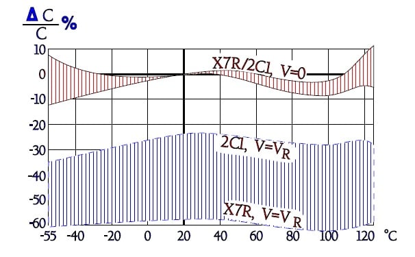
Figure C2-96. Typical curve range for capacitance versus temperature in X7R/2C1, with and without rated voltage applied.
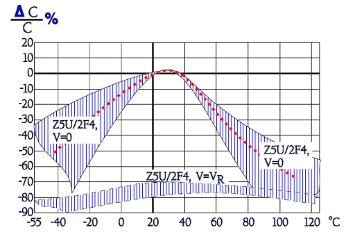
Figure C2-97. Typical curve range for capacitance versus temperature in Z5U/2F4, with and without rated voltage applied.
Tan δ versus temperature
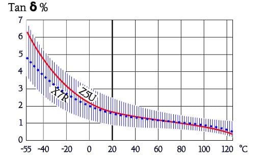
Figure C2-98. Typical curve ranges and average curves for Tan δ versus temperature in X7R/2C1 and Z5U/2F4.
IR versus temperature
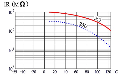
Figure C2-99. Typical examples of the IR versus temperature in ceramic chips.
The insulation resistance in Class 2 ceramic capacitors decreases with on average one power from room temperature to +125°C.
C 2.11.7 Frequency dependencies
Capacitance and Tan δ versus frequency
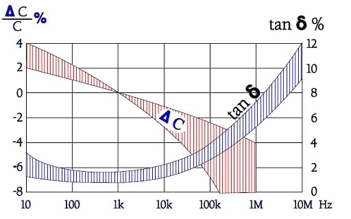
Figure C2-100. Typical curve ranges for capacitance and Tan δ versus frequency in X7R and 2C1 ceramics.
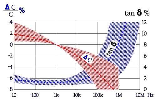
Figure C2-101. Typical curve ranges and average lines for capacitance and Tan δ versus frequency in Z5U / 2F4 ceramics.
Impedance and ESR versus frequency
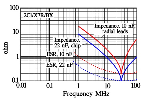
Figure C2-102. Examples of impedance and ESR versus frequency in X7R and 2C1 ceramics.

Figure C2-103. Other examples of the frequency dependence for impedance and ESR.

Figure C2-104. Examples of the frequency dependence of impedance and ESR in 2F4/Z5U ceramics.
C 2.11.8 Failure modes
See failure modes in section C2.9.2, Ceramic capacitors in general here. Just let us remember of the importance of avoiding temperature gradients in the ceramic during soldering processes, especially concerning SMDs. Repair with exchange of chips requires extra great care.
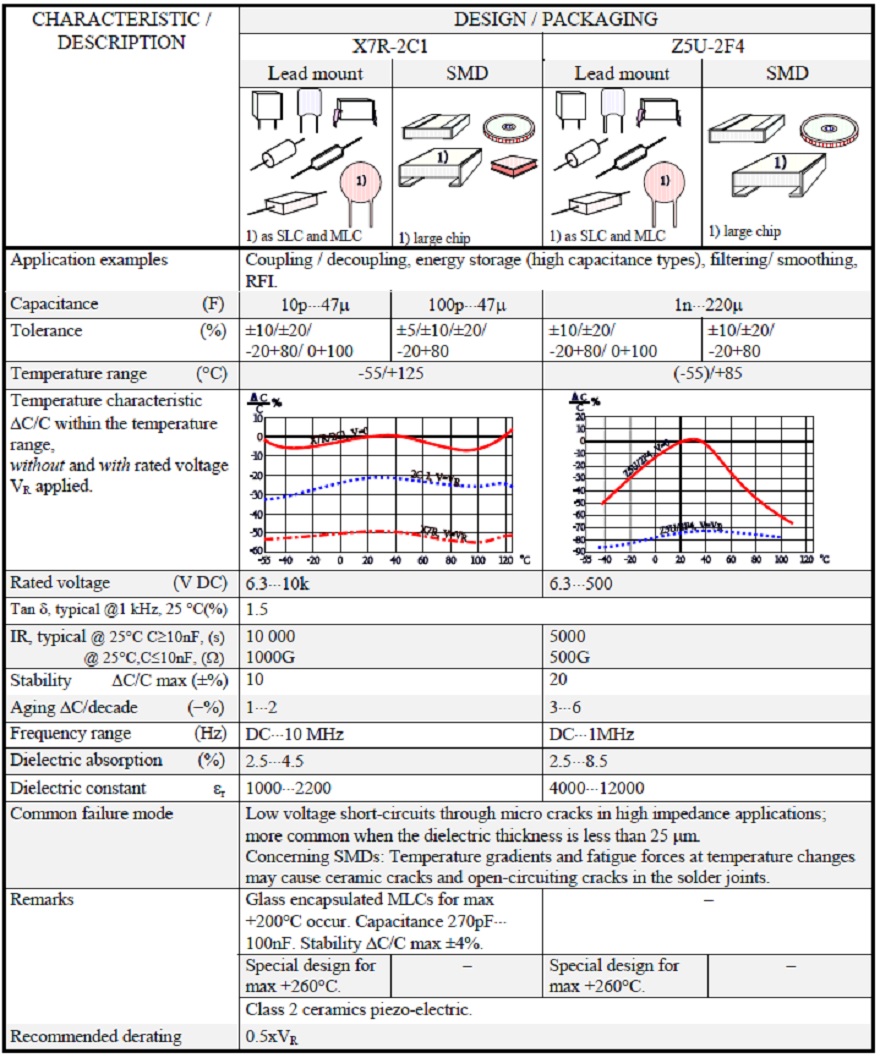
Table C2-13. CERAMICS CLASS 2 / X7R-2C1 / Z5U-2F4