
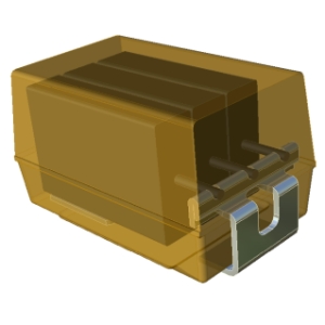
Solid Tantalum Capacitors with Manganese Dioxide and Polymer Electrolytes
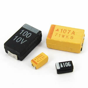
The most common types are SMD chip tantalum capacitors with solid electrolyte.
C 3.6 SOLID SINTERED TANTALUMS with MANGANESE DIOXIDE
C 3.6.1 Introduction
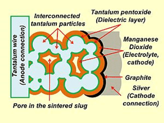
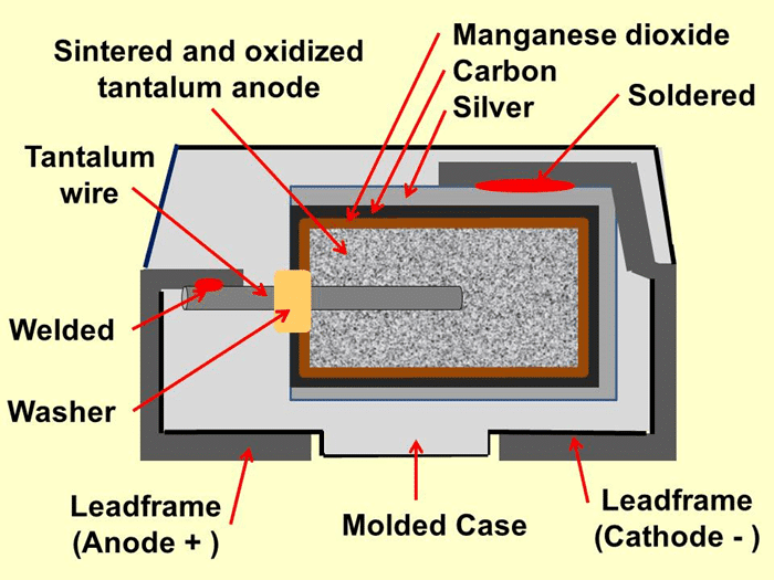
We start with cross section schematics of typical SMD tantalum chip construction.
The tantalum metal has a dielectric constant of approximately 27. The price for solid tantalums is relatively high due to mainly the high cost of the tantalum powder. The solid electrolyte theoretically has no limitations in operation and storage time. The capacitance range extends up to some thousands µF. The capacitors are characterized by a high CV product per volume unit, especially when high CV powders above 200k CV/g are introduced for low voltages and above 80k CV/g for higher voltages.
The conventional solid electrolyte is MnO2, however conductive polymer types are more and more favorite due to its lower ESR and reduced ignition features. On the other hand the MnO2 types are more robust against thermo-mechanical stress, stable electrical parameters under high temp & high humid environment, thus high reliability and longer operation life time applications still uses mostly established reliability MnO2 types as the main tantalum solid capacitor technology.
Physically, the capacitor also has a high density. Thus, lead mounted components always should be fixed mechanically against their substrate. Just as solid Al electrolytics this type requires large margins to the forming voltage that usually amounts to 2 to 4 times VR. For automotive and other high reliability applications ratios higher than 4 is required while for consumer electronics the ratio around 2 may be quite sufficient. The higher ratio favors not only higher reliability but also a better capacitance stability.
On the other hand higher VF/VR ratios means a correspondingly lower volumetric efficiency (capacitance is inversely proportional to the dielectric thickness). The maximum VR stops at 125 V DC for capacitors with polymer electrolyte and 100V DC for MnO2 types. However derating rules are different. It is recommended to derate MnO2 types by 50% for current surge circuits (directly on battery or DC/DC input) and 20% for non-high surge current applications (DC/DC output, timing, coupling/decoupling …). Tantalum polymer derating is recommended 10% for up to 16V capacitors and 20% for >16V capacitors for all kind of applications.
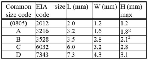
The capacitance stability is good (∆C/C ≤ ± 5%) and the tolerances range from (±5) ±10% to ±20%. The reverse voltage should, at a maximum 85 °C be limited to the least value of the alternatives: 10 % of VR or 1V. The continuous reverse voltage operation is not recommended, however small uneven spikes, such as diode overshoot voltage is acceptable. Chip designs are becoming very common and are well documented, with a functioning international standardization some basic case sizes have been established. However the market need and manufacturers feedback was faster then standardization and there are number of other case variants with different letter codes per manufacturing that may be very confusing in some cases – as the same letter from one manufacturer has different dimensions to the other.
As an example AVX X case is 1.5mm low profile variant of standard D case 7343 chip (AVX X case is equivalent to Kemet’s W case), however Kemet X case is a taller 4.3mm variant of standard D case 7343 part. (Kemet X case is equivalent to AVX E case).
The case size variants from manufacturers on market is in fact so wide that they are now using nearly complete alphabet options and began to use also numbers or combination of letters and numbers for different case size dimensions. The following table shows the common few sizes of a series that has acquired international acceptance under the same letter code:
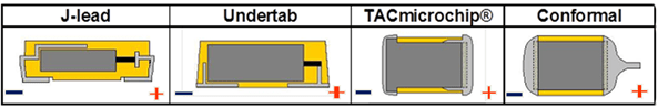
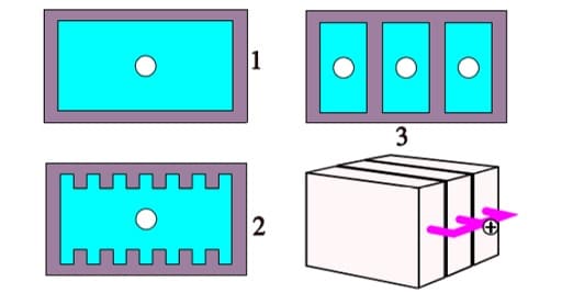
SMD Chip Construction Variants
The most common construction design shown on figure C3-46 above is called J-lead type as per the termination shape. There are also some other construction designs on the market – see figure C3-46b below.
- J-lead – most common, cost effective tantalum capacitor design with J-lead robust termination that works like a springs absorbing mechanical shocks and vibrations
- Undertab (facedown) – termination placed at the bottom of the case. This allows high density board mounting (no solder on capacitor sides) and also maximize its energy density / maximum capacitance and CV by inner space for larger anode. It does not allow solder quality visual inspection so this solution is not preferred by high rel applications.
- Diced design – such as TACmicrochip on figure below – proprietary AVX construction combining tantalum wafer and dice through technology allowing miniaturization down to 0201 case size. Diced designs are available also by other vendors such as Kemet/NEC or Vishay – most in combination with undertab configuration to maximize its CV.
- Conformal – original Spraque design – Vishay/Nichicon (AVX now) of dipped coated tantalum anodes. Advantage is in large, high CV anode, unmolded package is however not so flat with potential high speed pick and place issues.
C 3.6.2 Failure modes, Burn-in, Acceleration Factor (AF) and Derating
At first it has to be said that tantalum capacitors have been developed are representing one of the most reliable capacitor technology, historically linked with high rel applications. Nevertheless, solid tantalums sometimes are randomly stricken by short circuits. If the circuit has a high impedance it may happen that the failure disappears. A kind of self-healing has occurred. This is called sometimes a “scintillation”. Under certain conditions this kind of self-healing may occur also in circuits where the impedance is low. The reasons for this type of failure have been the subject of comprehensive researches and tests. After the forming the oxide film contains a number of weak sites caused by impurities in the tantalum metal or at sites of crystalline defects. If a voltage is applied gradually these sites will be the place for local higher currents that generated heat and heal the defect site. This is true for both MnO2 and conductive polymer while the mechanisms and effectiveness are different.
The local current generates a heat that creates temperatures in the micro spot of 400 to 500 °C. At that temperature the manganese dioxide in the case of MnO2 types is reduced to a lower degree of oxide (Mn2O3) with a several orders of magnitude higher resistivity. An insulating “patch” is formed over the leakage site, the local leakage current is choked and the capacitor self heals. This type of self-healing is provoked during the production phase by a voltage load, a so called voltage aging, that for every eliminated leakage site successively forces the leakage current down.
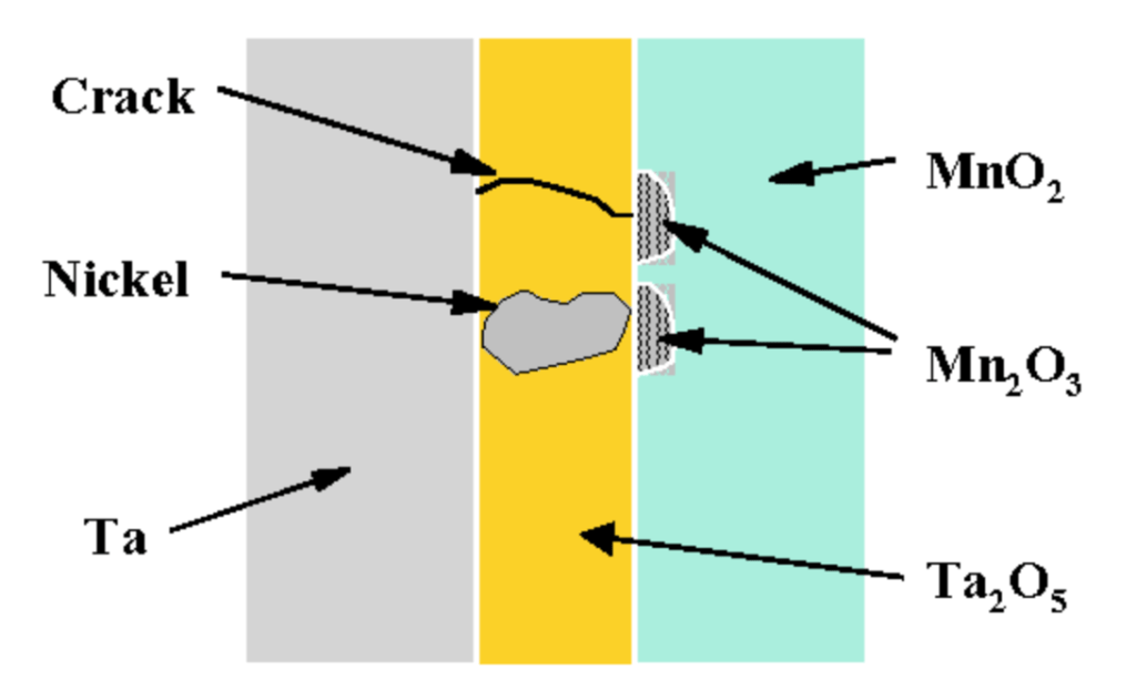
tantalum MnO2 Capacitors self-healing process
MnO2 self-healing considerations:
- microscopic localized mechanism with “no” influence to Capacitance, ESR
- “no” impact to DCL
- 100% hard surge current screening mandatory for ESA/MIL
- self healing and capacitor recovery may be limited in combination of following factors:
- high circuit resistance circuits >100kOhm
- aggressive reflow (=higher thermal damage to dielectric)
- very high derating >70%
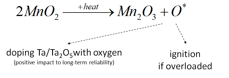
MnO2 Tantalum Capacitors Design Considerations
While tantalum self-healing process is bringing high reliability for the MnO2 based tantalum capacitors, the ignition if-overloaded, pose an important point for a careful evaluation of its circuit applications. The following are general guidelines regarding the application of Ta-MnO2 capacitors:
- Use series resistance – if applicable: limiting the external current available to a fault greatly reduces the chance of a fault site reaching the critical ignition temperature. Historically a series resistance of 1 to 3 ohms per applied volt has been recommended, this is not any more required. Modern designs may not tolerate this much ESR, and larger devices may contain sufficient electrical energy when charged to self-ignite should a fault suddenly appear. In these cases, de-rating and device screening are particularly important.
- Derate voltage: Derating is the most effective way to increase steady-state reliability, derate to 50% of rated voltage, and as much as 70% when series resistance is extremely low, on the order of 0.01 ohm per applied volt or less. If currents are externally limited – in low/no surge applications, 20% derating may be sufficient.
- Burn-in carefully: Many tantalum failures occur on first power up of an assembled device, as a result of assembly-induced dielectric faults. Facilitating successful self-healing through gradual application of voltage via a current-limited source may avert some of these failures. Subsequent exposure to maximum expected electrical and environmental stresses will serve as a proof test, since Ta-MnO2 capacitors that survive a given set of stresses once are likely to survive them almost indefinitely.
- Limit transient current: Current flows in excess of the manufacturer’s stated surge current limit are to be avoided, including those arising from non-routine events, such as hot-plugging of batteries or power supplies, short-circuit faults of system outputs, etc. In absence of a surge current specification, a value Imax<Vrated/(1+ESR) has been suggested.
- Observe ripple current/temperature limits: Ripple current ratings are typically based on the amount of ripple required to produce a given rise in device temperature above ambient. Excepting cases where the resulting waveforms would violate voltage or surge current limits, ripple current limits are a thermal management issue. Evaluate the test conditions under which the datasheet ripple limit figures are specified, and adapt those limits according to actual application conditions.
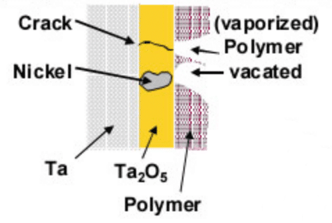
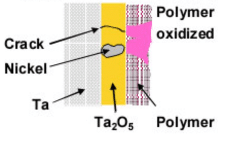
There is some self-healing effect also on tantalum polymer types as due to the high spot temperature the conductive polymer may evaporate / peel off (delaminate) or oxidize to high insulating state, thus the failure spot is eliminated. In effect, the capacitor reduce its high leakage through the defective site. In comparison, the self-healing on MnO2 is still considered as more effective, especially at lower current. On the other hand the self-healing in MnO2 parts is releasing some free oxygen that may extend the ignition failure mode. This is also one of the reason for higher derating (50%) of MnO2 types for high current circuit applications.
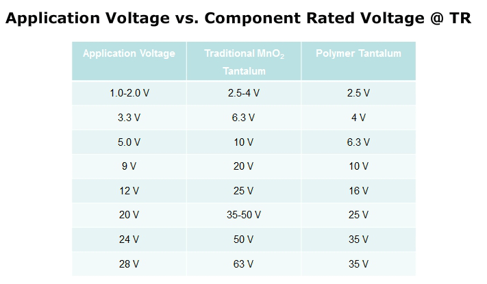
Polymer capacitors are much more robust against ignition and surge failures compare to MnO2 types. It is thus also reflected in its application derating recommendations usually as low as 10% up to 16V capacitors and 20% for >16V. See below applied voltage vs component rated voltage recommendation table:
polymer self-healing by evaporation
polymer self-healing by oxidization
tantalum polymer capacitor self-healing mechanisms
As long as such a capacitor operates in circuits with a high impedance (≥ 1-3 Ω/V) nothing will happen in these leakage sites except for, possibly, a further voltage aging. The reliability is high and often expressed in a number of fit, i.e., the quantity of failures per 109 hours. Should, however, the capacitor operate in a low impedance circuit (< 1-3Ω/V) with a correspondingly small time constant, it may be subjected to high charge and discharge currents. The local current density in a leakage site then may rise the temperature so much in the tantalum pentoxide that it is transformed from an amorphous to a crystalline form.
Because the crystalline form is inducing more conductive path, the part has a short-circuit. If the current is not cut off the temperature will rise further in the damage site until the tantalum pentoxide cracks. In that case the short-circuit conditions are aggravated. On the other hand, if the current is cut off before the short-circuit thermally degenerates the capacitor, a new careful voltage load may cause a selfhealing.
Unfortunately the crystalline form has a lower density than the amorphous one. It means that the crystalline failure site will expand to some extent and sooner or later will cause a secondary crack, a new short-circuit, etc. With continuous improvement, however, the quality of powder has significantly improved by reduction of impurities that are one of the major source of failures. Together with development of new, high quality processes on side of manufacturers, the latest tantalum capacitors shows much better reliability numbers compare to the past that enable new high CV parts introduction or changes in derating rules and formation/operation voltage ratios OR release of special series with reduced leakage current, higher surge robustness, industrial grade etc.
Despite of the improvements the basic physic law still applies and failure rate increases when the circuit impedance decreases below 1-3Ω/V. If we normalize the failure rate by taking the value at 3Ω/V as reference the result looks like the one in Figure C3-43. If we disregard the improvements in the last years and want to ensure having components that can be used in low impedance circuits, they should be subjected to a burn-in treatment where prospective defectives are weeded out and the voltage aging continues for a considerable time. We call the treatment a static burn-in. As a starting point for description of all such treatments usually MIL-C-39003, § 4.7.3 is stated. It is called just voltage aging.
There is prescribed a voltage load with minimum VR at 85 °C for at least 40 hrs and with a circuit impedance of 3 Ω. If we raise the voltage the processes are accelerated. Above all this is used when the failure rate level shall be established. MIL-C-39003, § 4.7.25 states how solid tantalums follow a stress function, very conformable to law, that depends on the ratio of applied voltage/rated voltage VDC/VR. The stress function is called Acceleration factor (AF) and follows, according to MIL-C-39003 the equation:
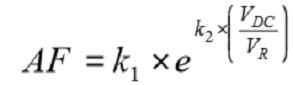
- k1 = 7.03412025*10-9
- k2 = 18.77249321
If we, for example, apply 1.2xVR the formula gives an AF of 43, i.e., 43 times more rapid results than if we test at VR. MIL-C-39003 limits the AF to maximum 20 000 which occur at an applied voltage of 1.5276 x VR.

The acceleration factor also is used for reliability prediction testing where the test time is “prolonged” by the AF. If the test time is called “t” and the number of tested components is N the number of component test hours will be AF x t x N. The product rapidly approaches such quantities that results ranging from 1 failure per 105 h to 1 failure per 109 h (1 fit) easily are predicted with a satisfactory confidence level. Theoretically, the specified 40 hours in MIL-C-39003 could be shortened by using the acceleration factor. AF = 1000 gives a corresponding test time of approximately 2.5 minutes. AF = 20 000 corresponds to approximately 7 seconds.
Of course, such accelerations won’t do for reliability prediction purposes. Other methods for increasing the test acceleration is by increasing the burn-in temperature to 125 °C and lower the circuit impedance further. One major manufacturer describes, in a technical article, a burn-in treatment at 125 °C for 12 hours, VDC > VR and the total circuit impedance ≤ 0.1 Ω/V. The manufacturer shows failure rates less than 1 fit (1 failure per 109 hours). Other manufacturers execute burn-in treatments at 125 °C by successively increased voltage pulses + discharges for some seconds. This is, however, another kind of burn-in that we shall deal with later.
It is not only remaining impurities that can cause short circuits in solid tantalums. In section C 1.4.3, about electrostatic force action, we previously showed with the help of formula C1-22 how voltage-loaded thin dielectrics are exposed to large pressures. If the voltage is now applied abruptly the dielectric is exposed to a mechanical shock. Under section C 3.1.4, solid electrolytes, we called the attention to those small slits that arise between the solid electrolyte and the dielectric. These voids can be reduced by repeated refilling operations of the solid electrolyte. The more complete the filling up, the higher the structural strength of the dielectric system, the higher capacitance per volume unit and the higher the price…
If we need capacitors which have to operate in low impedance circuits a static burn-in treatment is necessary. If the capacitor will be subjected to surge currents or high ripple it must also pass a dynamic burn-in. In the latter case it is important to choose designs where the manufacturer by choice of powder type and electrolyte filling procedures creates a low ESR. From Figure C3-48 we can read a failure rate decrease of between 5 and 12 times when the circuit impedance increases from ≤ 0,1 to ≥ 3Ω/V. A considerably much larger benefit can be attained by derating. Following diagram shows typical connections between derating, temperature and relative failure rate.
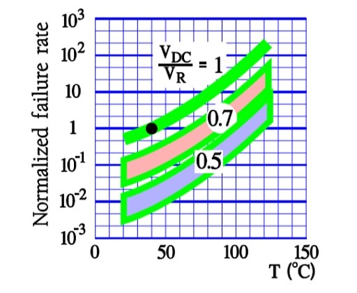
From Figure C3-48 it follows that a derating to 50 % of VR reduces the failure rate to approximately 0.5 % of the λ value at full rated voltage!
C 3.6.3 ESR reduction
ESR can be reduced by change of MnO2 solid electrolyte to more conductive polymer material, however there are also other ways to reduce ESR by change of the construction and anode shape.
From Figure C3-48 we also gather a decreasing failure rate when the temperature drops. Because the heat generation in an electric circuit is distributed proportionally to its resistances a reduction of the ESR in a capacitor leads to a corresponding decrease of its internal warming and thus its failure rate. Therefore styles with “ultra low” ESR values are developed. Especially Switched Mode Power Supplies (SMPS) demand ever-lower ESRs. Solid tantalums in SMD format are desired due to their high C/V ratio (capacitance C per unit volume V) which is of great interest to SMPS users.
One way to reduce the ESR is to shorten the current path to the capacitor elements in the center of a pellet. Several methods to achieve this are shown in the following schematic of different designs. In design example No. 2 the rough surface of the coated anode is covered with the outer silver paint. Compared to the conventional anode in design No. 1 the average distance between the equipotential silver paint plain and the dielectric is reduced which means a reduced ESR.
A further ESR reduction is achieved by dividing the tantalum pellet in several elements that are connected in parallel – so called multi anode technology – where the current paths are reduced considerably and the conductive paint surface is even larger than in design No. 2. The method is introduced in recent years and will certainly be developed further. Roughly the ESR is inversely proportional to the number of elements in parallel.
Note: When improvement of “ESR” is mentioned we mean ESR value measured at standard measurement conditions = 100kHz “high frequency” important for SMPS output capacitor performance. The multiple anode or rough anode design is in fact using a “skin” effect that improves ESR at higher frequences while ESR at lower freq. such as 120Hz is not impacted or slightly higher as it is driven mostly by dielectric losses.
The ESR (skin effect) depends also on the layers coating the manganese dioxide electrolyte or conductive polymer. First the buffer between the electrolyte and the silver paint, i.e., the carbon layer, then the silver paint that is bonded to the leadframe by a silver adhesive. Layer thickness and distribution, material and treatment during production, all contribute to a low ESR that has to remain low even after environmental exposure.
C 3.6.4 Reverse voltage
Solid tantalum electrolytics are considered as being able to stand more reverse voltage than wet electrolytics. The diode function in Figure C3-3 is in other words not equally evident. The diode in the equivalent circuit ought to be supplemented with a Zener-diode. What, then, the Zener voltage is varies according to certain short time investigations from 15 to 40% of VR, depending on lot and manufacturer. Long term investigations point to more conservative values. This is underlined by the fact that advanced powder technology has increased the sensitivity to reverse voltages. Some leading manufacturers may have different recommendations for reverse voltage. If nothing is said about reverse voltage limitations, we should for high reliability applications choose the least of applicable values from following alternatives:
EITHER
Temp. range & Derating
- -55/+25°C: 15% VR,
- +25→+55°C: 15%→ 10% VR,
- +55→+85°C: 10%→ 5% VR,
- +85→+125°C: 5%→ 1% VR,
OR
- of short duration maximum 1 V,
- continuous operations maximum 0.5 V
C 3.6.5 Tantalum Solid Capacitor Properties
Capacitance versus temperature

Capacitance versus frequency
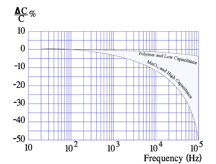
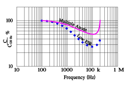
The higher the porosity and the finer the powder and worse conductivity (MnO2) the sooner the capacitor starts loosing capacitance due to the increasing time constant of the farthest in localized capacitor elements in the pellet. On the contrary, when the ESR is reduced the time constants decrease. That means that the so called capacitance roll-off is moved toward higher frequencies and the capacitance decrease will be correspondingly smaller. The effect of multianode is demonstrated in the following figure on MnO2 part that shows examples from 470 µF / 6.3 V tantalums of different designs. The impact of multianode construction for polymer tantalum is not so big change in capacitance vs frequency characteristics (as it is already more-less flat), but to the absolute ESR value.
ESR versus temperature
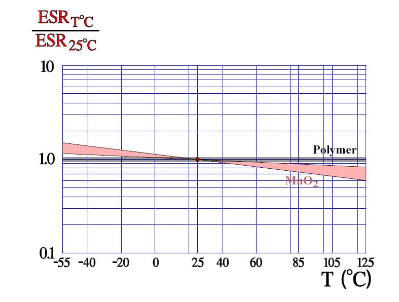
There is practically no ESR temperature dependence on polymer electrolyte and small dependence on manganese dioxide electrolyte.
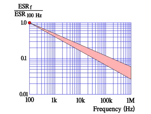
ESR versus frequency
Tan δ DF versus frequency

Note the difference in frequency dependence of the two loss characteristics ESR and Tan δ in Figures C3-54 and – 55. The influence of the linearly decreasing ESR in Figure C3-54 is visible at lower frequencies in Figure C3-55 but becomes more and more negligible when the frequency increases, just as the formula predicts: Tan δ = ESR x ωC.
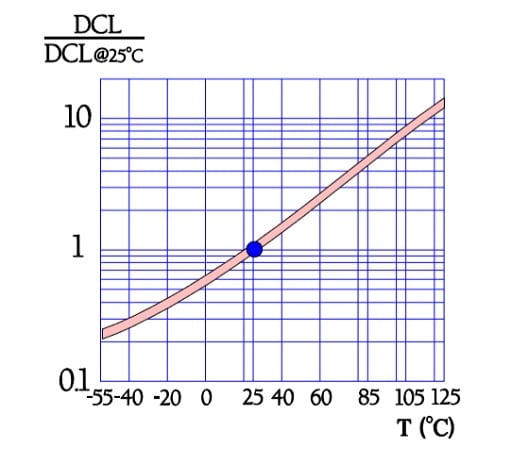
DCL Leakage current versus ambient temperature
The MnO2 DCL specification limit for standard parts is usually given as:
DCL = 0.01 x CV
,where C=capacitance, V=rated voltage … thus 100μF 10V MnO2 capacitor has a DCL standard limit as 10μA at rated voltage. In practice, by rule of thumb, typical leakage current is about ten times lower, so in real measurement we can expect DCL to be around 1μA for the 100μF 10V part.
The basic DCL leakage current level on MnO2 capacitors is typically 10x lower compare to the polymer capacitors. Thus for polymer tantalum capacitors, DCL specification limits follow:
DCL = 0.1 x CV
the 100μF 10V polymer capacitor has a DCL standard limit as 100μA and typically we can measure around 10μA at room temperature.
Important note is that due to the continuous improvement leakage current limits may be specific to series and manufacturer. Low leakage series or consumer highest CV series (with higher DCL) are available on the market that differ with DCL specification limits to the above general equations. It is always a good idea to check the manufacturer specification datasheet.
Normalized DCL leakage current plot as shown in Fig C3-56 is valid for both MnO2 and polymer types, however the absolute DCL values differ !
Leakage current versus voltage

The figure C3-57 above shows drop of the DCL with applied voltage (valid for both MnO2 and polymer types). By rule of thumb, DCL drop in one range with 50% derating. So taking an example of the 100μF 10V MnO2 capacitor with a DCL limit as 10μA at 10V rated voltage, we can assume the maximum leakage current values as 1μA at 5V applied and typical values would be around 0.1μA.
Leading manufacturers are providing now high fidelity simulation tools, where electrical characteristics of CAP, ESR, IMP, DF, DCL and S-parameters can be followed for individual capacitor part number. Here in alphabetical order: